STM32开发笔记51:STM32F4+DP83848以太网通信指南系列(五):MAC+DMA配置

本文是STM32F4开发系列的第五部分,详细介绍了如何配置STM32F407的MAC层和DMA以实现与DP83848的以太网通信。内容涵盖GPIO初始化、MAC层初始化、中断配置和网络服务启动,提供了一系列初始化函数的实现和来源解析。

摘要生成于 C知道 ,由 DeepSeek-R1 满血版支持, 前往体验 >

本章为系列指南的第五章,讲述STM32F407上MAC层以及其DMA的配置。我们在第一章知识储备章节说到,STM32F407会在168MHz主频之外分配一定的时间释放总线数据用来处理DMA,这其中就包含MAC层的DMA,复习一下STM32F4的总线架构图,(图片来自RM0090ST中文STM32F4手册P50):

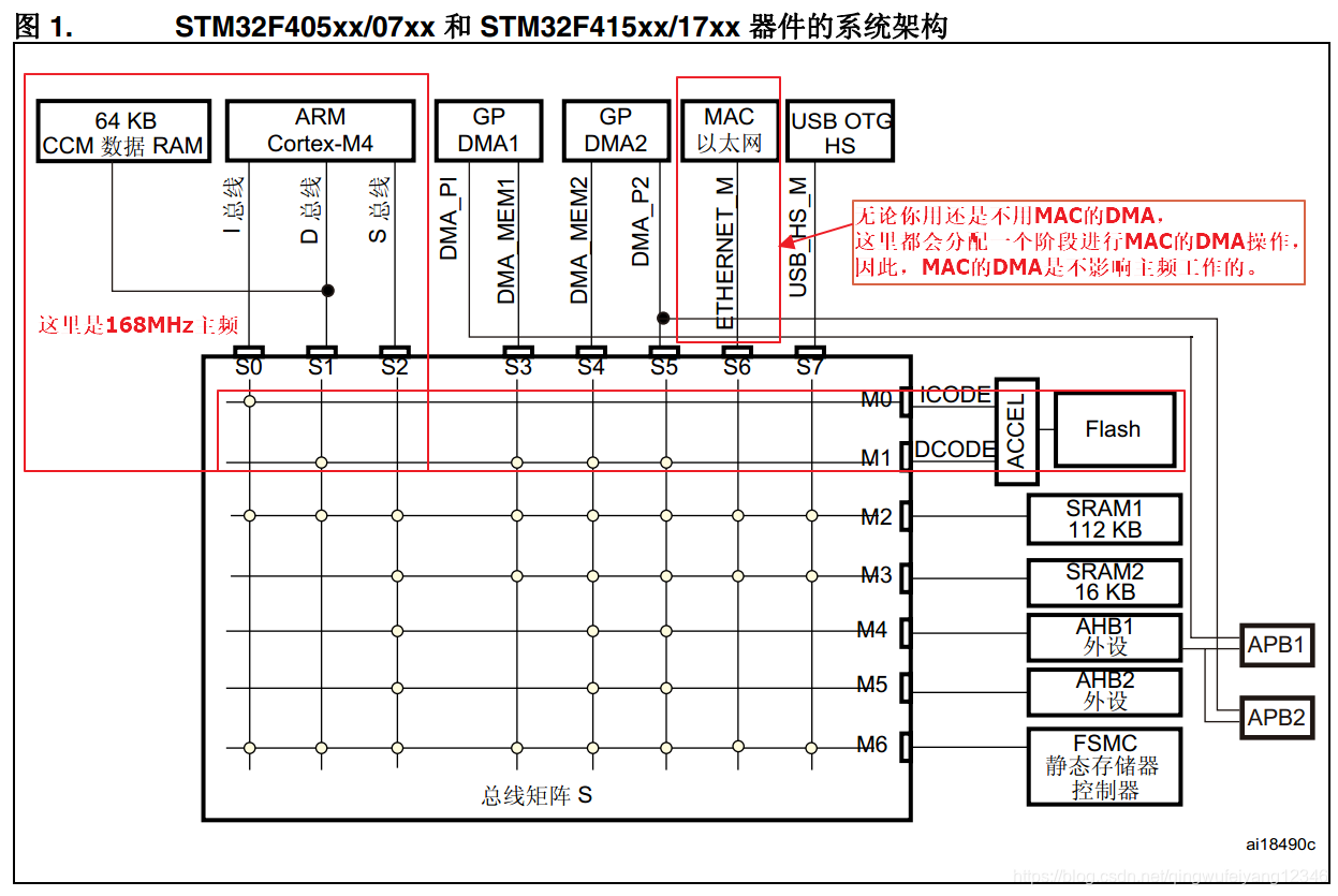
我们看到,在上图红框标注的的S6阶段,就是MAC层的DMA总线,CPU会在核心逻辑之外,有专门的时间片轮转周期处理这一阶段的DMA,所有的数据读写都是DMA来控制,不需要我们在核心逻辑中编写。

本章的要解决的任务只有一个:能编写一个自己构建的DP83848Init()函数,就像任何类似的UARTInit(),DelayInit()等函数一样,在main()函数初始化阶段调用,完成一系列启动网卡的操作。这个任务看似简单,其实比较复杂,因此本章篇幅也会比较多。这个函数包含多个子任务:

GPIO的初始化

MAC层及DMA配置

中断配置

网络服务启动

一、GPIO初始化

这个我们在上一章已经完成了。

二、MAC层初始化

2.1 编码

首先编写以下函数:

static void ETH_MACDMA_Config(void) {
    ETH_InitTypeDef ETH_InitStructure;

    /* Enable ETHERNET clock  */
    RCC_AHB1PeriphClockCmd(RCC_AHB1Periph_ETH_MAC | RCC_AHB1Periph_ETH_MAC_Tx | RCC_AHB1Periph_ETH_MAC_Rx, ENABLE);

    ETH_DeInit(); /* Reset ETHERNET on AHB Bus */

    ETH_SoftwareReset();   /* Software reset */

    while (ETH_GetSoftwareResetStatus() == SET);  /* Wait for software reset */

    /* ETHERNET Configuration
     * Call ETH_StructInit to get a default structure
     * if you don't like to configure all ETH_InitStructure parameter
     */
    ETH_StructInit(Ð_InitStructure);

    /* Fill ETH_InitStructure parametrs */
    /*------------------------   MAC   -----------------------------------*/
    ETH_InitStructure.ETH_AutoNegotiation = ETH_AutoNegotiation_Enable; /* 10M/100M自适应 */

    ETH_InitStructure.ETH_LoopbackMode = ETH_LoopbackMode_Disable;
    ETH_InitStructure.ETH_RetryTransmission = ETH_RetryTransmission_Disable;
    ETH_InitStructure.ETH_AutomaticPadCRCStrip = ETH_AutomaticPadCRCStrip_Disable;
    ETH_InitStructure.ETH_ReceiveAll = ETH_ReceiveAll_Enable; /* 混杂模式 */
    ETH_InitStructure.ETH_BroadcastFramesReception = ETH_BroadcastFramesReception_Enable;
    ETH_InitStructure.ETH_PromiscuousMode = ETH_PromiscuousMode_Disable;
    ETH_InitStructure.ETH_MulticastFramesFilter = ETH_MulticastFramesFilter_Perfect;
    ETH_InitStructure.ETH_UnicastFramesFilter = ETH_UnicastFramesFilter_Perfect;
    ETH_InitStructure.ETH_ChecksumOffload = ETH_ChecksumOffload_Enable; /* 在IP包收发时使用硬件计算校验和 */

    /*------------------------   DMA   -----------------------------------*/

    /* When we use the Checksum offload feature, we need to enable the Store and Forward mode:
    the store and forward guarantee that a whole frame is stored in the FIFO, so the MAC can insert/verify the checksum,
    if the checksum is OK the DMA can handle the frame otherwise the frame is dropped */
    ETH_InitStructure.ETH_DropTCPIPChecksumErrorFrame = ETH_DropTCPIPChecksumErrorFrame_Enable;
    ETH_InitStructure.ETH_ReceiveStoreForward = ETH_ReceiveStoreForward_Enable;
    ETH_InitStructure.ETH_TransmitStoreForward = ETH_TransmitStoreForward_Enable;

    ETH_InitStructure.ETH_ForwardErrorFrames = ETH_ForwardErrorFrames_Disable;
    ETH_InitStructure.ETH_ForwardUndersizedGoodFrames = ETH_ForwardUndersizedGoodFrames_Disable;
    ETH_InitStructure.ETH_SecondFrameOperate = ETH_SecondFrameOperate_Enable;
    ETH_InitStructure.ETH_AddressAlignedBeats = ETH_AddressAlignedBeats_Enable;
    ETH_InitStructure.ETH_FixedBurst = ETH_FixedBurst_Enable;
    ETH_InitStructure.ETH_RxDMABurstLength = ETH_RxDMABurstLength_32Beat;
    ETH_InitStructure.ETH_TxDMABurstLength = ETH_TxDMABurstLength_32Beat;
    ETH_InitStructure.ETH_DMAArbitration = ETH_DMAArbitration_RoundRobin_RxTx_2_1;

    /* 
     * 初始化时,RJ45变压器如果没有上电,ETH_Init会返回非0值,
     * 为确保系统上电后正确初始化网络,需要每500ms尝试初始化一次PHY,直到成功
     * DP83848_PHY_ADDRESS为上一章分析并定义的0x01
     */
    while( !ETH_Init(Ð_InitStructure, DP83848_PHY_ADDRESS) ) {
        vu32 sdelay = 84000000;
        while(sdelay--);
    }

    /* Enable the Ethernet Rx Interrupt */
    ETH_DMAITConfig(ETH_DMA_IT_NIS | ETH_DMA_IT_R, ENABLE);
}

上面的代码,配合注释虽然简单明了,但如果你直接copy到项目中编译,肯定会出现大把的错误,显然,从第一个结构体的定义就找不到,下面还有很多ETH的函数也找不到,那么,这个ETH_InitTypeDef结构体,以及下面ETH_DeInit()、ETH_SoftwareReset()、ETH_StructInit()等函数在哪里呢?

2.2 stm32f4x7_eth.c文件和Ethernet库函数

在第一章知识储备中,已经说过了,STM32F4标准库中并未带有ETH方面的库函数,在STM32官网搜索LWIP能够搜索到官方使用LWIP的DEMO,官方文档编号是STSW-STM32070,在这份文档中有LWIP协议栈,并且有官方的调用样例,我们可以从中挖掘到ETH部分的库函数。这份文档解压后,在/STM32F4x7_ETH_LwIP_V1.1.1/Libraries/STM32F4x7_ETH_Driver路径下面的stm32f4x7_eth.c以及配套的.h和一个stm32f4x7_eth_conf_template.h文件是比较关键的,类似于标准库提供的那些I2C,UART,SPI等库函数文件。我们将这三个文件全部引入工程,并且重命名stm32f4x7_eth_conf_template.h为stm32f4x7_eth_conf.h,所有配置均保持跟官方一致的默认配置,这样在本文2.1章节提到的结构体和那些ETH函数,就有定义了,编译起来也不会出错了。有了官方DEMO的样例文件,我们回过头来看一下2.1章节中出现的一大段初始化MAC层的代码,并不是我原创自己想当然瞎写出来的,我们可以考证一下其出处。

打开STM32F4x7_ETH_LwIP_V1.1.1\Project\Standalone\udp_echo_client\src\stm32f4x7_eth_bsp.c文件后,你会发现有相似的代码描述,我们看懂注释后,可以做适当的配置调整。

三、中断配置

这个环节相对比较简单,直接编码:

void ETH_NVIC_Config(void) {
    NVIC_InitTypeDef   NVIC_InitStructure;

    /* Enable the Ethernet global Interrupt */
    NVIC_InitStructure.NVIC_IRQChannel = ETH_IRQn;
    NVIC_InitStructure.NVIC_IRQChannelPreemptionPriority = 1;
    NVIC_InitStructure.NVIC_IRQChannelSubPriority = 0;
    NVIC_InitStructure.NVIC_IRQChannelCmd = ENABLE;
    NVIC_Init(&NVIC_InitStructure);
}

ETH_IRQn宏定义是STM32库中现成的ETH中断描述,中断优先级配置的1-0,相对比较高,但仍留了一位优先级给系统定时器中断排在前面。现在来回顾一下,目前我们已经拥有三个准备好的函数,分别是ETH_GPIO_Config()、ETH_MACDMA_Config()和ETH_NVIC_Config,第一个函数在上一章编写好的,后面两个是刚刚编写的。下面封装一个总体函数:

void ETH_BSP_Config(void) {
    ETH_GPIO_Config();

    ETH_NVIC_Config();      // Config NVIC for Ethernet

    ETH_MACDMA_Config();    // Configure the Ethernet MAC/DMA
}

以上,所有代码皆在stm32f4x7_eth_bsp.c文件中。

四、网络服务启动

我们现在已经完成了大部分的初始化和配置任务,下面,我们需要着手编写以太网服务的启动工作代码,也就是我们这一章节的核心任务,编写DP83848Init()函数:

void DP83848Init(uint8_t* HWADDR){
    int i;
    /* Configure ethernet (GPIOs, clocks, MAC, DMA) */
    ETH_BSP_Config();

    /* initialize MAC address in ethernet MAC */
    ETH_MACAddressConfig(ETH_MAC_Address0, HWADDR);
    /* Initialize Tx Descriptors list: Chain Mode */
    ETH_DMATxDescChainInit(DMATxDscrTab, &Tx_Buff[0][0], ETH_TXBUFNB);
    /* Initialize Rx Descriptors list: Chain Mode  */
    ETH_DMARxDescChainInit(DMARxDscrTab, &Rx_Buff[0][0], ETH_RXBUFNB);

    /* Enable the TCP, UDP and ICMP checksum insertion for the Tx frames */
    for(i = 0; i < ETH_TXBUFNB; i++) {
        ETH_DMATxDescChecksumInsertionConfig(&DMATxDscrTab[i], ETH_DMATxDesc_ChecksumTCPUDPICMPFull);
    }
    ETH_Start();
}

其中,ETH_BSP_Config()来自于我们上一阶段封装好的函数,其余的调用依然来自stm32f4x7_eth.c文件。虽然这里的注释描写得也十分清晰的了,这里有一点需要提一下,在上述代码的第9行和第11行就是配置了两个DMA的链状描述符,关于链状DMA描述符和环装DMA描述符,如果需要理解得更多一点,可以观看原子哥的视频教程,那里面花了一些篇幅介绍,不过我个人感觉视频中讲的也不是特别清楚,视频下载地址:https://pan.baidu.com/s/1jIvvTcy,暂时我们先这么用吧。

按照惯例,上面那一段函数也不是我突发奇想,心血来潮,闭着眼睛毫无根据写下的,我们来看看这段函数的出处,依然在之前那份LWIP文档里面,路径为:STM32F4x7_ETH_LwIP_V1.1.1\Utilities\Third_Party\lwip-1.4.1\port\STM32F4x7\Standalone\ethernetif.c,看第76行low_level_init()函数,顾名思义,low_level_init()就是底层初始化的意思,我们重点观察这个函数的后半部分,前面操作netif结构体的部分我们暂时用不到,后面部分调用ETH库函数的函数就是我们需要的。代码截取如下:

static void low_level_init(struct netif *netif)
{
#ifdef CHECKSUM_BY_HARDWARE
  int i; 
#endif
  /* set MAC hardware address length */
  netif->hwaddr_len = ETHARP_HWADDR_LEN;

  /* set MAC hardware address */
  netif->hwaddr[0] =  MAC_ADDR0;
  netif->hwaddr[1] =  MAC_ADDR1;
  netif->hwaddr[2] =  MAC_ADDR2;
  netif->hwaddr[3] =  MAC_ADDR3;
  netif->hwaddr[4] =  MAC_ADDR4;
  netif->hwaddr[5] =  MAC_ADDR5;

  /* initialize MAC address in ethernet MAC */ 
  ETH_MACAddressConfig(ETH_MAC_Address0, netif->hwaddr); 

  /* maximum transfer unit */
  netif->mtu = 1500;

  /* device capabilities */
  /* don't set NETIF_FLAG_ETHARP if this device is not an ethernet one */
  netif->flags = NETIF_FLAG_BROADCAST | NETIF_FLAG_ETHARP;

  /* Initialize Tx Descriptors list: Chain Mode */
  ETH_DMATxDescChainInit(DMATxDscrTab, &Tx_Buff[0][0], ETH_TXBUFNB);
  /* Initialize Rx Descriptors list: Chain Mode  */
  ETH_DMARxDescChainInit(DMARxDscrTab, &Rx_Buff[0][0], ETH_RXBUFNB);

#ifdef CHECKSUM_BY_HARDWARE
  /* Enable the TCP, UDP and ICMP checksum insertion for the Tx frames */
  for(i=0; i<ETH_TXBUFNB; i++)
    {
      ETH_DMATxDescChecksumInsertionConfig(&DMATxDscrTab[i], ETH_DMATxDesc_ChecksumTCPUDPICMPFull);
    }
#endif

   /* Note: TCP, UDP, ICMP checksum checking for received frame are enabled in DMA config */

  /* Enable MAC and DMA transmission and reception */
  ETH_Start();

}

顺便提一下,ethernetif.c这个源文件本身我们是不需要的,我们并不需要LWIP库中的任何代码,所有的一切都是借鉴其网络收发包模块是怎么编写的。

最后,我们再次小结一下,经过不断的对照和参考,我们现在已经有一份完整的DP83848Init()函数,这个函数将放在main()函数开头部分进行整个PHY、MAC、DMA的配置和初始化。

至此,我们这一章的任务就圆满完成了,我尽量做到每一行代码都有其出处,而不是只贴出代码,让读者只知其然不知其所以然,我想我们弄清楚这些出处后,就可以清晰地根据自己的不同设备和场景来移植。


National_Semiconductor的一款网络芯片的技术手册。1.0 Pin Descriptions m 9 1.1 Serial Management Interface 9 1.2 MAC Data Interface .9 1.3 Clock Interface 11 1. 4 LED Interface 1.5 Reset and Power down 12 1.6 Strap Options 12 1.7 10 Mb/s and 100 Mb/s PMD Interface 14 1.8 Special Connections 14 1. 9 Power Supply Pi 14 1. 10 Package Pin AsSi 15 2.0 Configuration 16 2. 1 Auto-Negotiation g 16 2.1.1 Auto-Negotiation Pin Control 16 2.1.2 Auto-Negotiation Register Control 16 2.1.3 Auto-Negotiation Parallel Detection 2. 1. 4 Auto-Negotiation Restart 2.1.5 Enabling Auto-Negotiation via Software 17 2.1.6 Auto-Negotiation Complete Time 17 2.2 Auto-MDIX 2. 3 PHY Address 18 2.3.1 Mll Isolate mode 2.4 LED Interface 19 2.4.1LED 19 2.4.2 LED Direct Control 2.5 Half Duplex VS Full Duplex 20 2.6 Internal Loopback 20 2.7 BIST 20 3.0 Functional Description .I.I... 21 3.1 Mll Interface 3.1.1 Nibble-wide mll data Interface 21 3.1.2 Collision detect 3.1.3 Carrier Sense 21 3.2 Reduced mll Interface 3.3 10 Mb Serial Network Interface(SNI) .22 3. 4 802.3u Mll Serial Management Interface 3.4.1 Serial Management Register Access 3.4.2 Serial Management Access protocol 22 3.4.3 Serial Management Preamble Suppression 4.0 Architecture 24 4.1100BASE-TX TRANSMITTER .24 4.1. 1 Code-group Encoding and Injection 26 4.1.2 Scrambler 26 4.1 3 Nrz to nrzi Encoder 26 4.1. 4 Binary to MLT-3 Convertor 26 4.2100 BASE-T×RECEⅣVER 26 4.2.1 Analog Front Et 26 4.2.2 Digital Signal Processor 26 4.2.2.1 Digital Adaptive Equalization and gain Control 28 4.2.2.2 Base Line Wander Compensation 4.2.3 Signal detect 4.2.4 MLT-3 to nrzi Decoder 4,25 nrz to nrz 4.2.6 Serial to parallel 4.2.7 Descrambler 4.2.8 Code-group Alignment 4.29 4B/5B Decoder 4.2. 10 100BASE-TX Link Integrity Monitor ..30 42. 11 Bad ssD Detection .30 www.national.com Oo寸∞∞∞ 4.3 10BASE-T TRANSCEIVER MODULE 30 4.3.1 Operational Modes 30 4.3.2 Smart squelch 31 4.3.3 Collision Detection and sQE 4.3.4 Carrier Sense 31 4.3.5 Normal Link Pulse detection/Generation 4.3.6 Jabber function …32 4.3. 7 Automatic Link Polarity detection and correction .....32 4.3.8 Transmit and Receive Filtering ...32 4.3.9 Transmitter 4.3.10 Receiver 5.0 Design Guidelines 33 5. 1 TPI Network circuit ....33 5.2 ESD Protection 34 5.3 Clock In(X1) Requirements 34 5. 4 Power feedback circu 35 5.5 Power Down/Interrupt 35 5.5.1 Power down control mode ....35 5.5.2 Interrupt Mechanisms 5.6 Energy Detect Mode 36 6.0 Reset Operation..∴.∴∴∴.37 6.1 Hardware reset 6.2 Software reset 7.0 Register Block ,,,,,,,,,38 7. 1 Register definition 7.1.1 Basic Mode Control Register(BMCR) 7.1.2 Basic Mode Status Register(BMSR) 44 7.1.3 PHY Identifier Register #1 (PHYIDR1) 45 7.1. 4 PHY Identifier Register #2(PHYIDR2 ..45 7.1.5 Auto-Negotiation Advertisement Register(ANAR) .......45 7.1.6 Auto-Negotiation Link Partner Ability Register(ANLPAR) (BASE Page) 7.1.7 Auto-Negotiation Link Partner Ability Register(ANLPAR)(Next Page) 7.1.8 Auto-Negotiate Expansion Register (ANER) 7.1.9 Auto-Negotiation Next Page Transmit Register(ANNPTR) 7.2 EXtended Registers 50 7.2.1 PHY Status Register(PHYSTS 7.2.2 Mll Interrupt Control Register(MICR 52 7.2.3 MIl Interrupt Status and Misc. Control Register(MISR) 7.2.4 False Carrier Sense Counter Register(FCSCR) 7.2.5 Receiver Error Counter Register(RECR 7.2.6 100 Mb/s PCS Configuration and Status Register(PCSR) 55 7.2.7 RMII and Bypass Register(RBR) 7. 2. 8 LED Direct Control Register(LEDCR 7. 2. 9 PHY Control Register(PHYCR) .....57 7.2.10 10Base-T Status/Control Register(1OBTSCR) 58 7. 2.11 CD Test and BIST Extensions Register(CDCTRL1) 60 7. 2. 12 Energy Detect Control (EDCR) 6 8.0 Electrical Specifications 62 8.1 DC Specs 62 8.2 AC Specs .,,,,.,64 8.2.1 Power Up Timing 64 8.2.2 Reset Timing 8.2.3 Mll Serial Management Timing 8.2.4 100 Mb/s MIl Transmit Timing 8.2.5 100 Mb/s Mll Receive Timing ............67 8.2.6 100BASE-TX Transmit Packet Latency Timing 67 8.2.7 100BASE-TX Transmit Packet Deassertion Timing 8.2.8 100BASE-TX Transmit Timing(tr/F& Jitter) 8.2.9 100BASE-TX Receive Packet Latency Timing 70 8.2.10 100BASE-TX Receive Packet Deassertion Timing 70 www.national.com 8.2.11 10 Mb/s Mll Transmit Timing 71 8.2.12 10 Mb/s Mll Receive Timing 8.2.13 10 Mb/s serial Mode Transmit Timing 8.2.14 10 Mb/s serial Mode Receive timing 8.2.15 10BASE-T Transmit Timing (Start of Packet 73 8.2. 16 10BASE-T Transmit Timing(End of Packet 73 8. 2. 17 10BASE-T Receive Timing(Start of Packet) 8.2.18 10BASE-T Receive Timing(End of Packet 74 8.2.19 10 Mb/s heartbeat Timing 75 8.2.20 10 Mb/s Jabber Timing 8222 Auto-Negotiation Fast Link Pulse(FLP) Timing…、∴ 8.2.21 10BASE-T Normal Link Pulse Timing .....,,,,76 8.2.23 100BASE-TX Signal Detect Timing 8.2.24 100 Mb/s Internal loopback timing 8.2.25 10 Mb/s Internal Loopback Timing .78 8. 2.26 RMII Transmit Timing .79 8.2.27 RMII Receive Timing 82.28 Isolation Timing 81 8.2.29 25 MHz OUT Timing 81 8.2.30 100 Mb/s X1 to TX CLK Timing 82 9.0 Physical Dimensions∴∴ ■■■ 84 ww.national. com Oo寸∞∞∞ List of Figures Figure 1. DP83848C Functional Block Diagram..... Figure 2. PHYAD Strapping Example 18 Figure 3. AN Strapping and LED Loading Example 19 Figure 4. Typical MDC/MDIO Read Operation ......23 Figure 5. Typical MDC/MDIO Write Operation 23 Figure 6. 100BASE-TX Transmit Block Diagram ,,,,,,.,,.24 Figure 7. 100BASE-TX Receive Block Diagram 27 Figure 8. EIA/TIA Attenuation Vs Frequency for 0, 50, 100, 130&150 meters of CAt 5 cable...... 28 Figure 9. 100BASE-TX BLW Event ........ Figure 10. 10BASE-T Twisted Pair Smart Squelch Operation 31 Figure 11 10/100 Mb/s Twisted Pair Interface...,.......... 33 Figure 12. Crystal Oscillator Circuit 34 Figure 13. Power Feeback Connection 35 www.national.com List of tables Table 1. Auto-Negotiation Modes .16 Table 2. PHY Address Mapping Table 3. lEd Mode select 19 Table 4. Supported packet sizes at +/-50ppm +/-100ppm for each clock Table 5. Typical MDIO Frame Format Table 5. 4B5B Code-Group Encoding/Decoding Table 6. 25 .,34 Table7.25 MHz Oscillator Specification∴.∴.∴ ,,,,,,,,,,34 Table 8. 50 MHz Oscillator Specification ,,35 Table 9. 25 MHz Crystal Specification Table 10 Register Map...................... 38 Table 11. Register Table ..∴......39 Table 12. Basic Mode Control Register (BMCR), address 0X00 Table 13. Basic Mode Status Register(BMSR), address 0x01 Tabe14. PHY ldentifier Register#1( PHYIDR1), address0x02.∴………………………4 Table 15 PHY Identifier Register #2 (PHYIDR2), address 0x03 45 Table 16. Negotiation Advertisement Register(ANAR), address 0x04 45 Table 17. Auto-Negotiation Link Partner Ability Register(ANLPAR)(BASE Page), address 0x05.... 46 Table 18 Auto-Negotiation Link Partner Ability Register(ANLPAR)(Next Page), address 0x05..... 48 Table 19. Auto-Negotiate Expansion Register(ANER), address 0X06 Table 20 Auto-Negotiation Next Page Transmit Register(ANNPTR), address 0x07 .∴.∴......,49 Table 21. PHY Status Register(PHYSTS), address 0x10 Table 22 Mll Interrupt Control Register(MICR), address 0x11 n..52 Table 23. MIl Interrupt Status and Misc. Control Register(MISR), address 0x12 .....∴.53 Table 24. False Carrier Sense Counter Register(FCSCR), address 0x14 54 Table 25 Receiver Error Counter Register(RECR), address 0x15 54 Table 26. 100 Mb/s PCS Configuration and Status Register(PCSR), address 0x16 Table 27. RMI and Bypass Register(RBR), addresses 0x17...................56 Table 28 LED Direct Control Register (LEDCR), address 0X18 量重面 重重m 56 Table 29 PHY Control Register(PHYCR), address Ox19 57 Table 30 10Base-T Status/Control Register(10BTSCR), address OX1A Table 31. CD Test and BIST Extensions Register(CDCTRL1), address 0x1B ..60 Table 32. Energy Detect Control (EDCR), address 0x1D ,,61 www.national.com Oo寸∞∞∞ In Layou 乙uzoOHOau PFBIN2 24 RBIAS 23上 PFBOU RX DV/MIL MODE AVDD33 CRS/CRS DV/LED CFG RESERVED RX ER/MDIX EN 41 RESERVED 42 RXD O/PHYAD1 DP838480 PFBIN1 RXD 1/PHYAD2 Td RXD 2/PHYAD3 TD RXD 3/PHYAD4 AGND OGND JOVDD33 Hz=z3oa au>u c u>uOu p vie NS Package Number Vbh48A www.national.com 1.0 Pin Descriptions The DP83848C pins are classified into the following inter- All DP83848C signal pins are i/o cells regardless of the face categories(each interface is described in the sections particular use. The definitions below define the functionality that follow of the l/O cells for each pin Serial Management Interface Input MAC Data Interface Output Clock Interface Type: I/o Input/Output LED Interface Type OD Open Drain Reset and power down Type: PD, PU Internal Pulldown/Pullup Strap Options Strapping Pin(All strap pins have weak in- --10/100 Mb/s Pmd Interface ternal pull-ups or pull-downs. If the default Special Connect Pins strap value is needed to be changed then an external 2.2 k resistor should be used Power and ground pins Please see Section 1.6 for details.) Note: Strapping pin option. Please see Section 1.6 for strap definitions 1.1 Serial Management Interface Signal Name Tvpe Pin t Description MDC 31 MANAGEMENT DATA CLOCK: Synchronous clock to the MDIo management data input/output serial interface which may be asynchronous to transmit and receive clocks. The maximum clock rate is 25 Mhz with no minimum clock rate MDIO 30 MANAGEMENT DATA l/O: Bi-directional management instruc tion/data signal that may be sourced by the station management entity or the PhY. This pin requires a 1.5k pullup resistor 1.2 MAC Data Interface Signal name Type Pin t Description TX CLK MII TRANSMIT CLOCK: 25 MHz Transmit clock output in 100 Mb/s mode or 2.5 MHz in 10 mb/s mode derived from the 25 mHz reference clock Unused in emil mode the device uses the x1 reference clock in put as the 50 MHz reference for both transmit and receive SNI TRANSMIT CLOCK: 10 MHZ Transmit clock output in 10 Mb SNI mode. The MAc should source TX EN and TXdO using this clock TX EN L PD Mll TRANSMIT ENABLE: Active high input indicates the pres ence of valid data inputs on TXD3: 0 RMII TRANSMIT ENABLE: Active high input indicates the pres- ence of valid data on TXD[1: 0 SNI TRANSMIT ENABLE: Active high input indicates the pres- ence of valid data on TXD 0 TXD 0 MII TRANSMIT DATA: Transmit data Mll input pins, TXD3: 0 TXD 1 3456 that accept data synchronous to the TX ClK (2.5 MHz in 10 Mb/s mode or 25 MHz in 100 Mb/s mode) TXD 2 RMII TRANSMIT DATA: Transmit data RMII input pins, TXD[1 TXD 3 S.L. PD that accept data synchronous to the 50 MHz reference clock SNI TRANSMIT DATA: Transmit data sNi input pin TXd 0, that accept data synchronous to the TX CLK (10 MHz in 10 Mb/s sni mode) www.national.com Oo寸∞∞∞ Signal name Type Pin #i Description RX CLK 38 MI RECEE CLOCK: Provides the 25 mhz recovered receive clocks for 100 Mb/s mode and 2.5 MHz for 10 Mb/s mode Unused in rmll mode the device uses the xl reference clock in put as the 50 MHz reference for both transmit and receive SNI RECEIVE CLOCK: Provides the 10 MHz recovered receive clocks for 10 Mb/s sni mode RXD∨ S.O. PD MII RECEIVE DATA VALID: Asserted high to indicate that valid data is present on the corresponding RXD[3: 0]. MIl mode by de fault with internal pulldown RMII Synchronous Receive Data Valid: This signal provides the RMII Receive Data valid indication independent of carrier sense This pin is not used in SNI mode RX ER S.O. PU MIl RECEIVE ERROR: Asserted high synchronously to RX CLK to indicate that an invalid symbol has been detected within a re ceived packet in 100 Mb/s mode RMII RECEIVE ERROR: Assert high synchronously to X1 when- ever it detects a media error and rxdv is asserted in 100 mb/s This pin is not required to be used by a mac, in either mil or rmll mode, since the Phy is required to corrupt data on a receive error This pin is not used in SNI mode RXD O S.O. PD MII RECEIVE DATA: Nibble wide receive data signals driven syn RXd 1 chronously to the rx clk, 25 Mhz for 100 Mb/s mode 2.5 MHZ for 10 Mb/s mode ) RXD[3 0] signals contain valid data when RXD 2 45 RX DV is asserted RXD 3 46 RMII RECEIVE DATA: 2-bits receive data signals, RXD[1: 0], driv en synchronously to the X1 clock, 50 MHZ SNI RECEIVE DATA: Receive data signal, RXD 0, driven syn chronously to the RX ClK RXd0 contains valid data when CRs is asserted. RXD[3: 1] are not used in this mode CRS/CRS DV S.O. PU MII CARRIER SENSE: Asserted high to indicate the receive me dium is non idle RMII CARRIER SENSE/RECEIVE DATA VALID: This signal combines the rmll carrier and receive data valid indications For a detailed description of this signal, see the RMII Specifica- SNI CARRIER SENSE: Asserted high to indicate the receive me dium is non -idle. It is used to frame valid receive data on the RXD 0 signal COL S.O. PU MI COLLISION DETECT: Asserted high to indicate detection of a collision condition(simultaneous transmit and receive activity) in 10 Mb/s and 100 Mb/s Half Duplex Modes While in 10BASE-T Half Duplex mode with heartbeat enabled this pin is also asserted for a duration of approximately 1 s at the end of transmission to indicate heartbeat (SQE test In Full duplex Mode, for 10 Mb/s or 100 Mb/s operation, this sig nal is always logic 0. There is no heartbeat function during 10 Mb/s full duplex operation RMII COLLISION DETECT: Per the RMll Specification, no COL signal is required. The MAc will recover CRS from the CRS DV signal and use that along with its tX en signal to determine col- SNI COLLISION DETECT: Asserted high to indicate detection of a collision condition(simultaneous transmit and receive activity) in 10 Mb/s sni mode www.national.com 10
评论 5
添加红包

请填写红包祝福语或标题

红包个数最小为10个

红包金额最低5元

当前余额3.43前往充值 >
需支付:10.00
成就一亿技术人!
领取后你会自动成为博主和红包主的粉丝 规则
hope_wisdom
发出的红包
实付
使用余额支付
点击重新获取
扫码支付
钱包余额 0

抵扣说明:

1.余额是钱包充值的虚拟货币,按照1:1的比例进行支付金额的抵扣。
2.余额无法直接购买下载,可以购买VIP、付费专栏及课程。

余额充值