


Run OpenSPARC T1 on CentOS (百度网盘)_Jude_99的博客-优快云博客
上一篇开博做了1.1 的解析,1.1 只是大概做了介绍,我高亮了一些关键信息,没什么好讲的。
这次讲1.2 节,英文好的,可以自己直接看。我会高亮并注解(#汉语注解在中间#)一些关键信息,并找到对应verilog源码做简单的解释。如果读者看过这三本书可以更好的理解:《计算机组成与设计 硬件/软件接口》《计算机体系结构-量化研究方法》,《超标量处理器设计》,当然不限于这三本,看过其他计算机体系结构和处理器设计的书也可以。
1.2 Functional Description
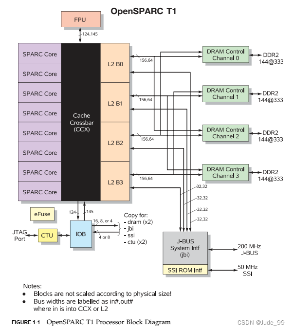
The features of the OpenSPARC T1 processor include:
■ 8 SPARC V9 CPU cores, with 4 threads per core, for a total of 32 threads #8核,每核4线程#
■ 132 Gbytes/sec crossbar interconnect for on-chip communication #132GB/s 的crossbar#
■ 16 Kbytes of primary (Level 1) instruction cache per CPU core #16kB 一级指令缓存#
■ 8 Kbytes of primary (Level 1) data cache per CPU core #8kB 一级数据缓存#
■ 3 Mbytes of secondary (Level 2) cache – 4 way banked, 12 way associative shared
by all CPU cores #3MB 二级缓存,4个bank, 共12路一起共享#
■ 4 DDR-II DRAM controllers – 144-bit interface per channel, 25 GBytes/sec peak
total bandwidth #4个DDR-II DRAM控制器,如果要上Zed Board,可以试着改为DDR3#
■ IEEE 754 compliant floating-point unit (FPU), shared by all CPU cores #浮点处理单元#
■ External interfaces:
■ J-Bus interface (JBI) for I/O – 2.56 Gbytes/sec peak bandwidth, 128-bit
multiplexed address/data bus #外部接口,后面再看#
■ Serial system interface (SSI) for boot PROM #boot PROM的接口,具体支持哪些PROM?#
FIGURE 1-1 shows a block diagram of the OpenSPARC T1 processor illustrating the
various interfaces and integrated components of the chip.
1.3 OpenSPARC T1 Components
This section provides further details about the OpenSPARC T1 components.
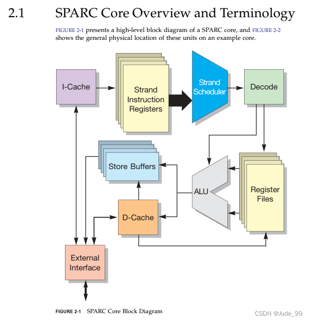
1.3.1 SPARC Core
Each SPARC core has hardware support for four threads #支持4线程的硬件#. This support consists of a
full register file (with eight register windows) per thread, with most of the address
space identifiers (ASI), ancillary state registers (ASR), and privileged registers
replicated per thread. The four threads share the instruction, the data caches, and the
TLBs. Each instruction cache is 16 Kbytes with a 32-byte line size #I cache 时讲#. The data caches are write through, 8 Kbytes, and have a 16-byte line size #D cache 时讲#. The TLBs include an autodemap feature which enables the multiple threads to update the TLB without
locking. #四个线程共享指令缓存,数据缓存和TLB,每个线程都有单独的寄存器组,大部分是地址空间标识,辅助状态寄存器,特权寄存器和TLB(translation lookaside buffers,可以理解为缓冲区),TLB有自动寻址功能,能够使多线程不被锁的更新TLB#
Each SPARC core has single issue, six stage pipeline.#每个核有单发射,6级流水线# These six stages are:
1. Fetch
2. Thread Selection
3. Decode
4. Execute
5. Memory
6. Write Back
FIGURE 1-2 shows the SPARC core pipeline used in the OpenSPARC T1 Processor.
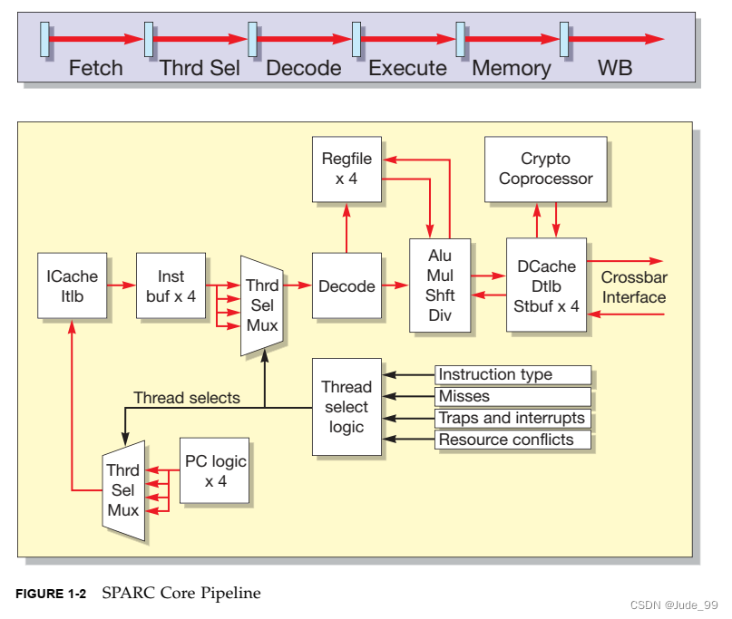
Each SPARC core has the following units:
1. Instruction fetch unit (IFU) includes the following pipeline stages – fetch, thread
selection, and decode. The IFU also includes an instruction cache complex.
2. Execution unit (EXU) includes the execute stage of the pipeline.
3. Load/store unit (LSU) includes memory and writeback stages, and a data cache
complex.
4. Trap logic unit (TLU) includes trap logic and trap program counters.
5. Stream processing unit (SPU) is used for modular arithmetic functions for crypto.
6. Memory management unit (MMU).
7. Floating-point frontend unit (FFU) interfaces to the FPU.
总结: 四个线程有各自的寄存器组,如下图的Strand Instauction Registers ,Register Files ,Store Buffers ,都有四份,其他的部分是公用的,通过每个线程的标识和优先级来选择对应线程的指令和数据。
边看边写,难免有错误或理解不到位的地方,欢迎留言指出,讨论。关于对应的代码还在看,之后会讲。


 被折叠的 条评论
为什么被折叠?
被折叠的 条评论
为什么被折叠?
 到【灌水乐园】发言


