


 本文介绍了逻辑门电路在计算机科学中的基础作用,包括AND、OR、NOT、XOR门的工作原理,以及它们的真值表。通过布尔代数简化逻辑表达式,并探讨了如何使用NAND门构建其他基本门电路。此外,还讲解了半加器和全加器的概念,用于实现二进制计算。D-latch作为数据存储元件,在没有输入时保持数据。
Introduction
logic gates are fundamental while essential to computer hardware. A logic gate can be featured multiple inputs but only leads to a single output.
Be careful! Boolean circuit wise, when we say "give a value", it means the logic gate produces a TRUE value. Logic True and logic False are physically represented by voltage - no or low voltage denotes False (0), and high voltage indicates True (1). Hence, give a value means "high voltage".
In the article, the terminologies 1s / 0s, high / low voltage, and give a value / not give a value will be used interchangeably. Additionally, the website we use to show logic gate is: Logic.ly https://logic.ly/demo/Feel free to have a play with it.
basic gates
AND gate

what is logic AND? It gives a value only when both inputs hold true, meaning that only for inputs (1, 1) does it produce 1. For example, you say: I own a extravagent mansion AND I am paid 100,000 pounds annually. So only when both conditions are satisfied, your statement is true.
OR gate

waht is logic OR? the logic gate produces 1 when at least one of all inputs is true, which indicates that input combinations (0,1), (1,0), and (1,1) can lead to a true value. For example, you tell a fairy: I want a high salary or a big house. She only needs to realise at least one of your wishes.
NOT gate

Not operation is unary and the simplest to learn. Given any value inputed, the gate returns a reversed output. For example you input 0 it outputs 1.
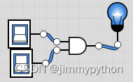
XOR gate
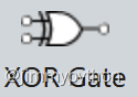
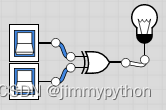
XOR stands for "excluded OR". It returns a value when either of the inputs is true. It can be represented by a combination of logic gates.
The combinational logic gate shown above simulates the functionality of a XOR gate. Some people may find it fairly complicated. Later on we will devise how these circuits are devised.
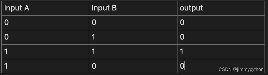
Truth table
Truth table is simply a table that enumerates all possible input combinations and the according output under the law of a basic/combinational logic gate.
truth table of AND gate
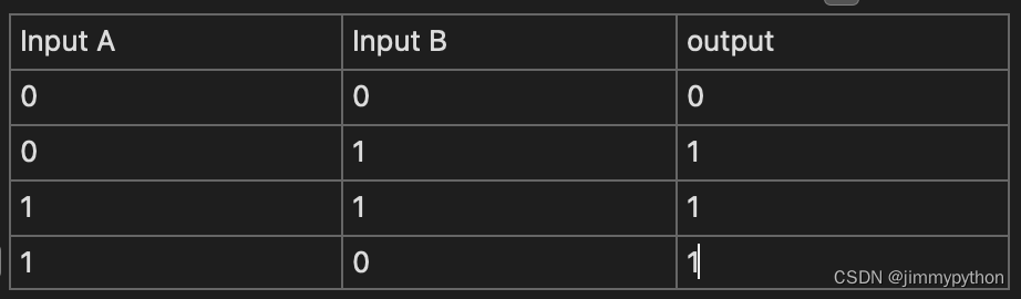
truth table of OR gate
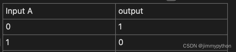
truth table for NOT gate
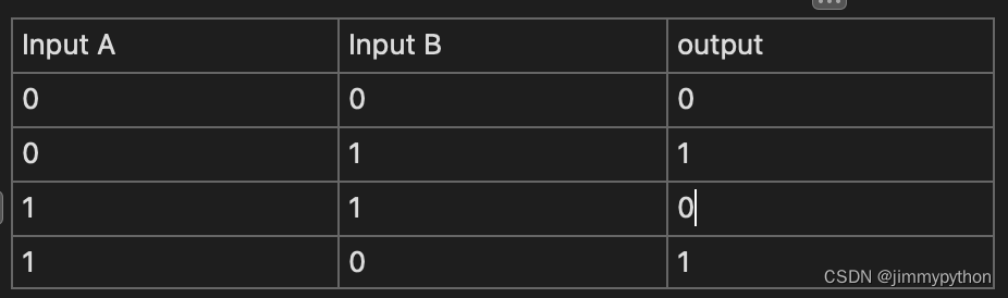
the truth table for XOR gate
truth table are usually used to build logic gate. How?
Inputs and intended output are entered for all possible values. We are to find the rows of inputs that make the output true. For example, in the truth table for XOR gate, we can see that the output will be true when input A is 0, B is 1, or when input A is 1, B is 0.
In the two valid pairs of inputs, we need to identify the input that is 0 and turn it to 1 by not gate, and use AND gate to connect the two inputs. For example, in the second row of the truth table of XOR gate, the input A is 0 while the input B is 1, then we do: !A*B; similarly, for the last row, we have A*!B.
Two possible combinations of inputs both return an output of 1, so we utilise OR gate to connect the two -- then we have the expression for XOR gate by OR, AND, and NOT gate: !A*B+A*!B.
However, usually, this is not the last step. Some more complicated boolean expressions can be simplified via certain techniques. It makes sure that we can use as few gates as possible to achieve the same function for cost-effective purposes.
Boolean Algebra
A AND B is represented as A*B, or A∧B, A&B which is logic multiplication, which makes sense in a set operation...
A OR B is A+B, A∨B, A|B which is logic addition
NOT A is usually represented as ¬A, Ā, 'A, !A
A XOR B is: A⊕B, A⊻B, A^B
similar to number operation, we do have some rules of arithmetics in boolean operation
general rules
A*0=0, A*1=1, A*A=A, A*~A=0
A+1=1, A+0=A, A+A=A, A+~A=1
A*B=B*A, A+B=B+A (commutative rules)
A+B+C=A+(B+C), A*B*C=A*(B*C) (associative rules)
A*(B+C)=A*B+A+C, A+(B*C)=(A+B)*(A+C) (distributive rules)
A+(A*B)=A, A*(A+B)=A (absorption rules) (proof: try (A*1)+(A*B) , the second equation can be transformed to the first)
~(A*B)=~A+~B, ~(A+B)=~A*~B (De Morgan) (can be proved via Venn diagram)
A=~~A (double negative)
Use the powerful internet if you want to prove some of them.
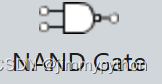
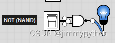
NAND gate
why do we sometimes use a combination of logic gates to represent another basic logic gate?
Mass production of a circuit costs less than producing all in a small amount. Thus, it's wise to use one circuit to represent the others. However, in some scenarios, representing a circuit by a combination of logic circuit is inefficient and would become too unnecessarily complicated.
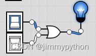
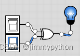
nand gate is the AND gate followed by a NOT gate. It is said that NAND gate can represent all the basic circuits.
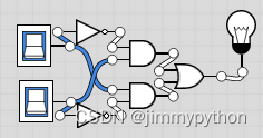
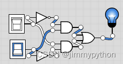
Use NAND gate to represent all the basic gates. How do we figure out why they make sense? use boolean algebra to prove it. Dont worry, it's quite easy!
XOR
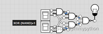
This is purely obtained from the boolean expression, by the truth table.
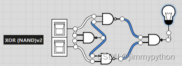
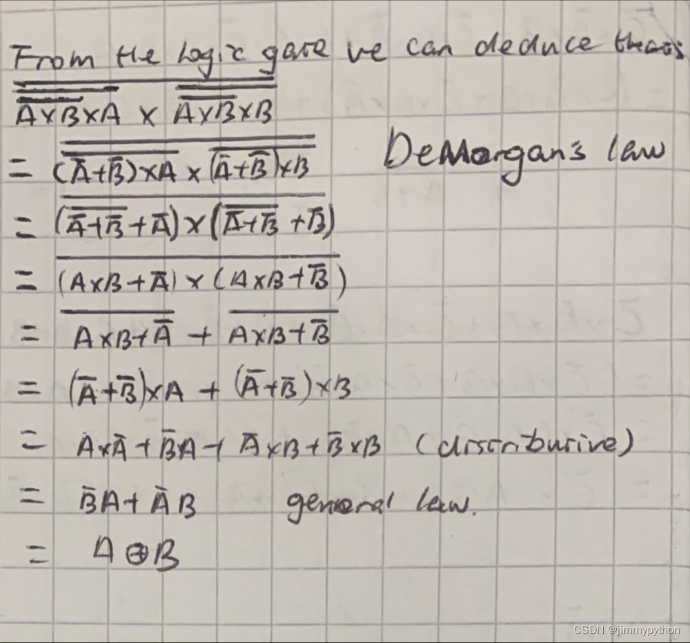
Notice that this one achieves the function with one less gate! this can be proved to function using boolean algebra. We firstly look at the gate above and use all possible combinations of inputs and correspond outputs to obtain a truth table, from which we can get a boolean expression. Then, it is simplified and turns out to be !A*B+A*!B.
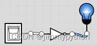
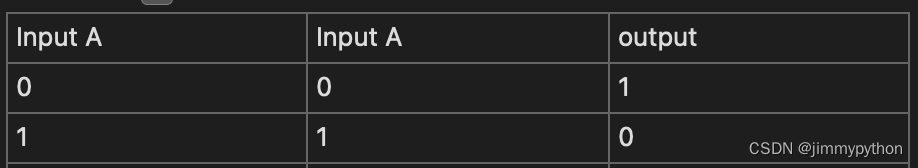
NOT
AND
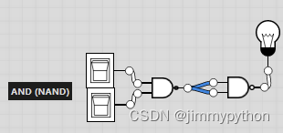
can you draw a truth table for it?
OR
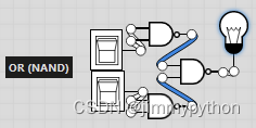
to prove this, we use De Morgan's law: !A*!B=!(A+B)
then: !(!A*!B)=!(!(A+B))
then: !(!A*!B)=A+B (double negative)
Useful circuits
half adder and full adder
The full adder is the combinational logic gate that enables the computer to calculate binary numbers physically.
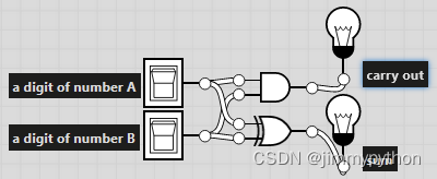
half adder
Half adder is a simplified version of a full adder. This is a machine that add one digit of one binary with another. How does it do addtion?
Assume that all of you have learnt about binary arithmetics.
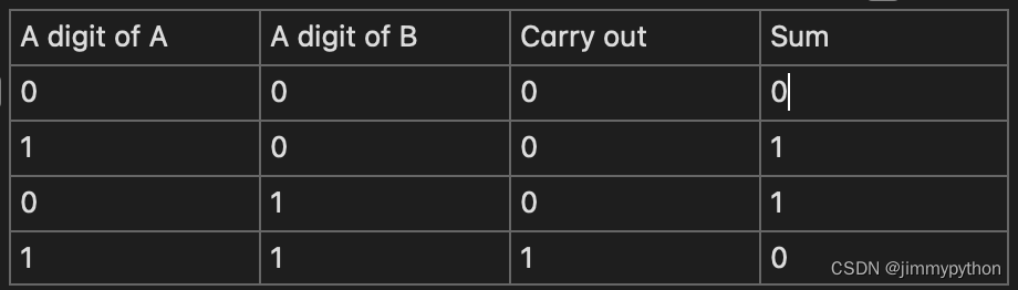
binary addtion, one digit
Here is a truth table that takes all possible combinations of inputs and produces intended outputs.
now we make a boolean expression that relates the digit of A and the digit of B to the output: A*!B + !A*B->Sum, A*B->Carry out. The first expression can be simplified to A⊕B. So, we make logic gates base on these expressions!
Full adder
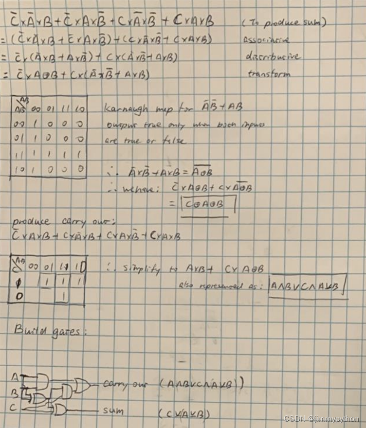
What if we want to calculate several digits? for example 10+11 (bin)? Then we need to consider the carry in.
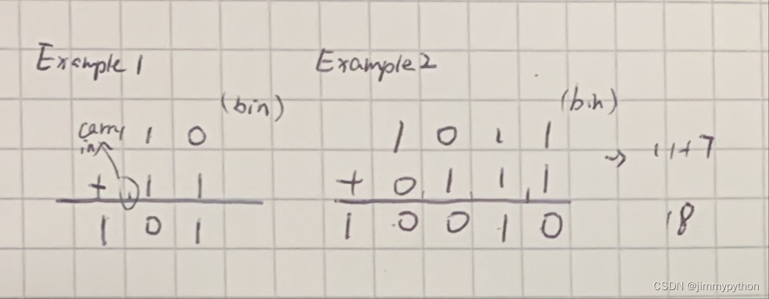
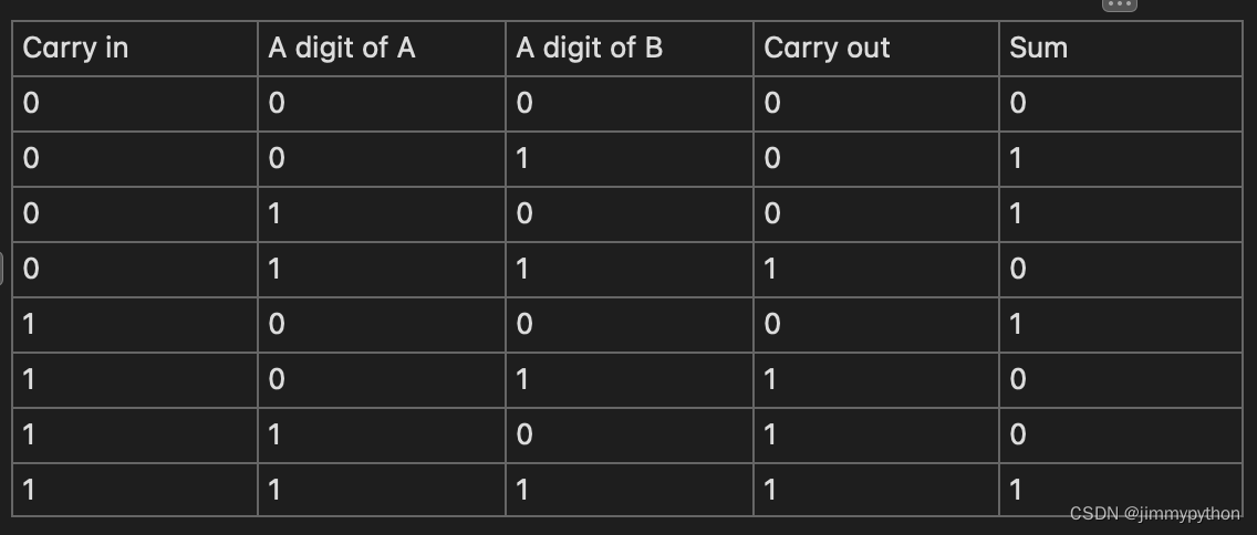
The truth table above shows all useful combinations of three inputs and according outputs. We make boolean expressions out of which and simplified it as usual. Note 'carry in' as C. For Sum, we have: !C*!A*B+!C*A*!B+C*!A*!B+C*A*B. For carry out, we have: !C*A*B+C*!A*B+C*A*!B+C*A*B
This is wayyyyy too complicated -- any factories who adopt this expression will bankrupt immdiately. If not, consumers suffer - opening a web page may need minutes, and the game design will be impractical attributed to its low computational performance.
so we need to simplify the boolean expressoin above!
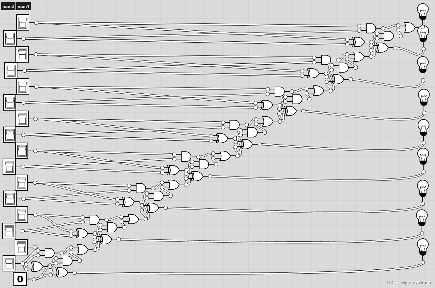
that's a one digit full adder. Usually, we use much bigger full adders with several bytes. Here is a 8-digit full adder (one byte)
D-latch
J-latch
The purpose of this D-latch is to store data when there is no current (input)
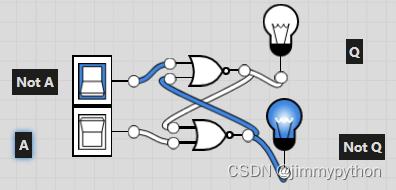
If you enter an input, it gives an ouput, which will hold on even if the input is turned off
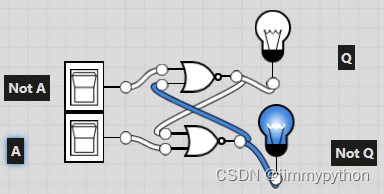
D-latch A-level version
Registers hold data temporarily and release them at regular time intervals according the clock speed. So we need to add a clock into this model so its change in output responses to the input and the clock.
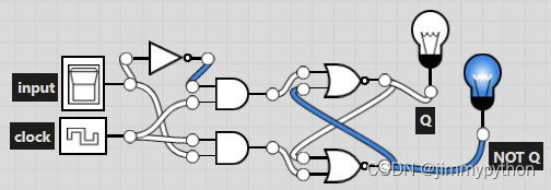
it is said to be a simplified version of a D-latch.


 178
178

 被折叠的 条评论
为什么被折叠?
被折叠的 条评论
为什么被折叠?
 到【灌水乐园】发言


