


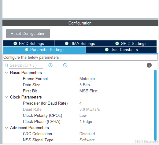
1.MX配置
支持spi mode0,时钟支持133mhz(max)
2.驱动
void FLASH1_CS_LOW()
{
    HAL_GPIO_WritePin(FLASH_CS2_GPIO_Port, FLASH_CS2_Pin, 0);
}
void FLASH1_CS_HIGH()
{
    HAL_GPIO_WritePin(FLASH_CS2_GPIO_Port, FLASH_CS2_Pin, 1);
}
void FLASH2_CS_LOW()
{
    HAL_GPIO_WritePin(FLASH_CS1_GPIO_Port, FLASH_CS1_Pin, 0);
}
void FLASH2_CS_HIGH()
{
    HAL_GPIO_WritePin(FLASH_CS1_GPIO_Port, FLASH_CS1_Pin, 1);
}

/*******************************************************************************
 * Function Name  : SPI_FLASH_SectorErase
 * Description    : Erases the specified FLASH sector.
 * Input          : SectorAddr: address of the sector to erase.
 * Output         : None
 * Return         : None
 *******************************************************************************/
void SPI_FLASH_SectorErase(u32 SectorAddr)
{
    uint8_t status = 0;
    /* Send write enable instruction */
    status = SPI_FLASH_WriteEnable();

    /* Select the FLASH: Chip Select low */
    FLASH1_CS_LOW();

    uint8_t cmd[4] = { 0 };
    cmd[0] = W25X_BlockErase;
    cmd[1] = (SectorAddr >> 16) & 0xff;
    cmd[2] = (SectorAddr >> 8) & 0xff;
    cmd[3] = SectorAddr & 0xff;

    (void) HAL_SPI_Transmit(&hspi1, cmd, 4, 0xffffffff);

    FLASH1_CS_HIGH();
    /* Wait the end of Flash writing */
    SPI_FLASH_WaitForWriteEnd();
}

/*******************************************************************************
 * Function Name  : SPI_FLASH_PageWrite
 * Description    : Writes more than one byte to the FLASH with a single WRITE
 *                  cycle(Page WRITE sequence). The number of byte can't exceed
 *                  the FLASH page size.
 * Input          : - pBuffer : pointer to the buffer  containing the data to be
 *                    written to the FLASH.
 *                  - WriteAddr : FLASH's internal address to write to.
 *                  - NumByteToWrite : number of bytes to write to the FLASH,
 *                    must be equal or less than "SPI_FLASH_PageSize" value.
 * Output         : None
 * Return         : None
 *******************************************************************************/
void SPI_FLASH_PageWrite(u8 *pBuffer, u32 WriteAddr, u16 NumByteToWrite,
                         u16 colmun)
{
    uint8_t status, end = 0;
    uint8_t cmd[4] = { 0 };
    uint8_t cmd1[4] = { 0 };
    /* Enable the write access to the FLASH */
    status = SPI_FLASH_WriteEnable(); //06

    /* Select the FLASH: Chip Select low */
    FLASH1_CS_LOW();

    /* Send "Write to Memory " instruction */
    cmd[0] = W25X_PageProgram;
    cmd[1] = (colmun >> 8) & 0xff;
    cmd[2] = colmun & 0xFF;
    HAL_SPI_Transmit(&hspi1, cmd, 3, 0xffffffff);
    HAL_SPI_Transmit(&hspi1, pBuffer, NumByteToWrite, 0xffffffff);
    FLASH1_CS_HIGH();

    FLASH1_CS_LOW();
    cmd1[0] = 0x10;//excute_cmd
    cmd1[1] = (WriteAddr >> 16) & 0xff;
    cmd1[2] = (WriteAddr >> 8) & 0xFF;
    cmd1[3] = (WriteAddr) & 0xff;
    HAL_SPI_Transmit(&hspi1, cmd1, 4, 0xffffffff);
    FLASH1_CS_HIGH();

    end=SPI_FLASH_WaitForWriteEnd();

}

void SPI_FLASH_BufferRead(u8 *pBuffer, u32 ReadAddr, uint32_t NumByteToRead,
                          u16 colmun)
{
    uint8_t status;
    u8 cmd[4] = { 0 };
    u8 cmd1[4] = { 0 };

    FLASH1_CS_LOW();
    cmd[0] = 0x13;
    cmd[1] = (ReadAddr >> 16) & 0xff;
    cmd[2] = (ReadAddr >> 8) & 0xff;
    cmd[3] = ReadAddr & 0xff;
    HAL_SPI_Transmit(&hspi1, cmd, 4, 0xffffffff);

    FLASH1_CS_HIGH();

    status= SPI_FLASH_WaitForWriteEnd();

    FLASH1_CS_LOW();
    cmd1[0] = 0x0b;
    cmd1[1] = (colmun >> 8) & 0xff;
    cmd1[2] = (colmun) & 0xff;
    cmd1[3] = 0;

    HAL_SPI_TransmitReceive(&hspi1, cmd1, pBuffer, NumByteToRead, 0xffffffff);
    FLASH1_CS_HIGH();
}

/*******************************************************************************
 * Function Name  : SPI_FLASH_ReadID
 * Description    : Reads FLASH identification.
 * Input          : None
 * Output         : None
 * Return         : FLASH identification
 *******************************************************************************/
u8 SPI_FLASH_ReadID(void)
{
    FLASH1_CS_LOW();
    uint8_t cmd[2] = { 0x9f, 0x00 };
    uint8_t buf[4] = { 0 };
    HAL_SPI_Transmit(&hspi1, cmd, 2, 0xffffffff);
    HAL_SPI_Receive(&hspi1, buf, 4, 0xffffffff);
    FLASH1_CS_HIGH();

    if ((buf[0] == 0x2c) && (buf[1] == 0x24))
    {
        return 1;
    }

    return 0;
}

/*******************************************************************************
 * Function Name  : SPI_FLASH_WriteEnable
 * Description    : Enables the write access to the FLASH.
 * Input          : None
 * Output         : None
 * Return         : None
 *******************************************************************************/
u8 SPI_FLASH_WriteEnable(void)
{
    uint8_t status;
    u8 data[1] = { 0 };

    do
    {

        FLASH1_CS_LOW();
        data[0] = 0x06;
        HAL_SPI_Transmit(&hspi1, data, 1, 0xffffffff);
        FLASH1_CS_HIGH();
        osDelay(1);
        status = readstatus(0xc0);

    }
    while ((status & 0x02) == 1);

    return status;
}

void flash1_reset(SPI_HandleTypeDef *hspi)
{
    u8 data[1] = { 0xff };
    if (hspi == &hspi1)
    {
        FLASH1_CS_LOW();
        HAL_SPI_Transmit(&hspi1, data, 1, 0xffffffff);
        FLASH1_CS_HIGH();
    }
    else
    {
        FLASH2_CS_LOW();
        HAL_SPI_Transmit(&hspi2, data, 1, 0xffffffff);
        FLASH1_CS_HIGH();
    }

}

/*******************************************************************************
 * Function Name  : SPI_FLASH_WaitForWriteEnd
 * Description    : Polls the status of the Write In Progress (WIP) flag in the
 *                  FLASH's status  register  and  loop  until write  opertaion
 *                  has completed.
 * Input          : None
 * Output         : None
 * Return         : None
 *******************************************************************************/
u8 SPI_FLASH_WaitForWriteEnd(void)
{
    u8 FLASH_Status = 1;

    /* Send "Read Status Register" instruction */
    do
    {
        FLASH_Status = readstatus(0xc0);
        osDelay(1);
    }
    while ((FLASH_Status | 0x02) == 0);

    return FLASH_Status;
}

uint8_t readstatus(uint8_t status)
{

    HAL_StatusTypeDef ret;
    FLASH1_CS_LOW();

    /* Send "Read Status Register" instruction */
    //  SPI_FLASH_SendByte(W25X_ReadStatusReg);
    uint8_t buf[4] = { 0 };
    uint8_t read[4] = { 0 };
    buf[0] = 0x0f;
    buf[1] = status;
    HAL_SPI_TransmitReceive(&hspi1, buf, read, 3, 0xffffffff);
    FLASH1_CS_HIGH();
    return read[2];
}

void flash1_unlock(uint8_t addr, uint8_t *cmd, uint8_t len)
{

    FLASH1_CS_LOW();

    uint8_t buf[6] = { 0 };
    buf[0] = 0x1f;
    buf[1] = addr;
    memcpy(&buf[2], cmd, len);
    HAL_SPI_Transmit(&hspi1, buf, len + 2, 0xffffffff);

    FLASH1_CS_HIGH();

}
3.闲谈
这个系列的flash还是第一次写驱动,读写都比较麻烦。(如果有错别杠,是我错了)
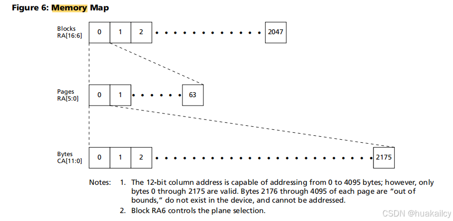
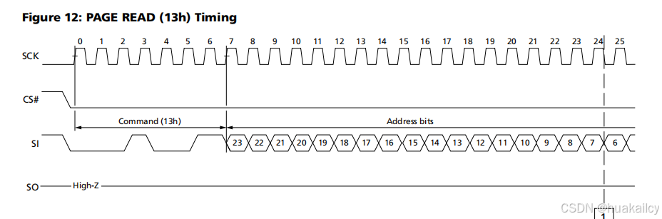
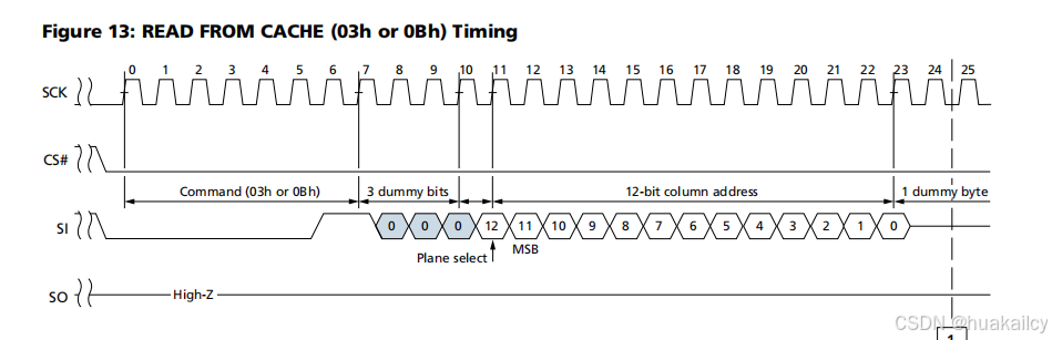
0.关于这个地址看了几遍总算明白了,(真的阴间),首先13h这个寄存器的24位address bit就是blocksRA+pagesRA,刚好17位+7位虚拟。其次就是03h寄存器的12位地址就是BytesCA的地址,弄清这个好办了;
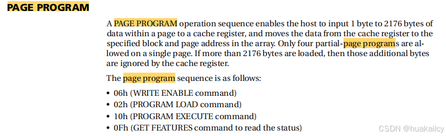
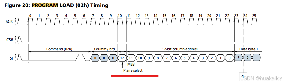
1.flash写的步骤,会先给你写进缓存寄存器,再写进数据寄存器,读的话,也是一样的。
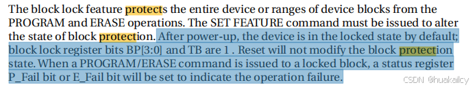
2.上电后,设备默认处于锁定状态;块锁寄存器位BP[3:0]和TB为1,如下图所示:
![]()
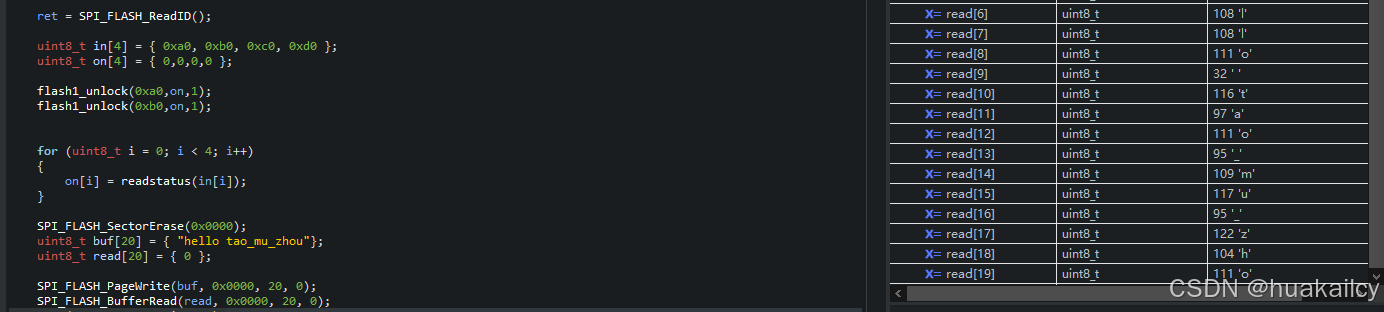
3.所以上电要对它进行解锁操作 flash1_unlock(),全部置0
![]()
4.记录一下整个操作:
5.巨坑点:2gb的是分为两个plane,奇数块和偶数块,这就是坑点了,他的12位缓存地址,外加一位区分奇数偶数块:plane select位,不然的话只能读偶数块,奇数块无法读取。


 被折叠的 条评论
为什么被折叠?
被折叠的 条评论
为什么被折叠?
 到【灌水乐园】发言


