


 本文详细介绍了在DE2开发板上实现Altera ChecksumMaster示例的过程,解决了原厂手册中步骤无法直接应用于DE2的问题,包括硬件设计调整及软件代码优化,最终实现了在SRAM上的成功运行。
Abstract
Checksum Master為Quartus II 7.2 Handbook Vol:4中,示範使用Component Editor將user logic包成component後,並撰寫software driver的範例,但手冊中的程式和步驟都無法在DE2上順利執行,本文提出解決的方法。
使用環境 : Quartus II 7.2 SP1 + Nios II 7.2 SP1 + DE2 (Cyclone II EP2C35F627C6)
手冊版本 :Quartus II Version 7.2 Handbook Volume4 : SOPC Builder
Introduction
Checksum Master是Altera在Quartus 7.1之後的範例程式,用以取代以前的PWM(pulse width modulator),PWM只示範了Avalon-MM slave interface,但Checksum Master同時示範了master和slave,且搭配SOPC Builder 7.1之後大改的介面。
不過很不幸的,Altera所附的範例和手冊中的步驟,僅適用於Altera原廠的版子,並不適用於DE2,經過幾天的搏鬥,總算修改成適用於Quartus 7.2 SP1和DE2的範例。
下載Checksum Master
我將Altera原廠的Checksum Master上傳了,請按此下載altera_avalon_checksum.zip。
原廠Checksum Master範例的問題
1.範例僅適用於Altera原廠的版子,並不適用於DE2。
2.範例中使用onchip memory,不過由於DE2上EP2C35F627C6 FPGA的logic element限制,onchip memory最多只能設定49K左右,但這樣的memory size仍無法執行此範例。
Solution
本文並沒有打算重寫整個tutorial,所以建議先將Quartus II 7.2 Handbook Vol.4 Ch.9 Developing Components for SOPC Builder瀏覽一次,在此只將與手冊中不適用於DE2之處列出。
1.使用DE2的reference design
在手冊中的P.9-9頁,Altera建議我們使用<Nios EDS install path>/examples/<verilog or vhdl>/<board version>/standard 目錄下的硬體,由於DE2用的是EP2C35F627C6這顆晶片,直覺會選Cyclone II的niosII_cycloneII_2c35這塊版子,但可惜這是Altera原廠的版子,並非DE2,若選擇這塊版子,Quartus II連編譯都不會過。
請在此下載DE2的reference design
http://www.terasic.com/downloads/cd-rom/de2/
根據你DE2的型號和使用Quartus II的版本,下載適當的DE2_System版本。
若你使用的是Quartus II 7.2,則建議下載Quartus II 7.1的版本,畢竟Quartus II 7.1大改,7.2和7.1較接近,遇到的問題會較少。
以我的狀況,是使用DE2_System_1.4b.zip這個版本。
DE2的Nios II reference design在壓縮檔內的
\DE2_demonstrations\SOPC_Builder\Reference_Design\DE2_NIOS\
將這個目錄複製到任何位置,並更改目錄名稱為checksum_master_onchip,使用Quartus II開起DE2_NIOS.qpf。
2.使用on-chip memory
在Quartus II Vol.4 Ch.9 P.9-24,有一段話,特別強調須使用on-chip memory。
 The test program uses an on-chip memory peripheral called onchip_ram. If your SOPC Builder system does not have an on-chip memory you should add an on-chip memory to the design. The test program requires that the name of the on-chip RAM and the component name used in the test program match. Connect the on-chip RAM to the Nios II data master.
當將on-chip memory加入DE2_NIOS後,儘管只是預設的4K,在Quartus II編譯也會有以下錯誤訊息:
Error : Cannot place all RAM cells in designError : Can't fit design in device
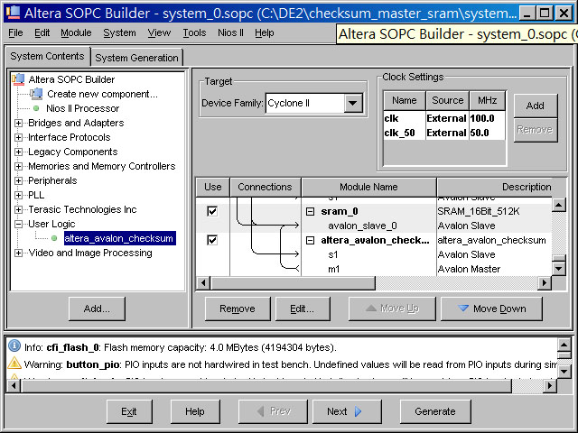
原因是on-chip memory相當浪費logic element count,FPGA已經塞不下了,或許你會說,『DE2的Nios II reference design放了很多我沒用到的component,將其刪除就可放on-chip memory了』,聽起來是個可行方案,我試著將component刪到只剩下最簡,Nios II CPU也改成最簡單的Nios II/e,如此可將on-chip memory擴大到49K,也依照了手冊的步驟加入了user logic component,最後SOPC Builder如下:
DE2 reference design完整code如下
DE2_NIOS.v
//
--------------------------------------------------------------------
//
Copyright (c) 2005 by Terasic Technologies Inc.
//
--------------------------------------------------------------------
//
//
Permission:
//
//
Terasic grants permission to use and modify this code for use
//
in synthesis for all Terasic Development Boards and Altera Development
//
Kits made by Terasic. Other use of this code, including the selling
//
,duplication, or modification of any portion is strictly prohibited.
//
//
Disclaimer:
//
//
This VHDL/Verilog or C/C++ source code is intended as a design reference
//
which illustrates how these types of functions can be implemented.
//
It is the user's responsibility to verify their design for
//
consistency and functionality through the use of formal
//
verification methods. Terasic provides no warranty regarding the use
//
or functionality of this code.
//
//
--------------------------------------------------------------------
//
//
Terasic Technologies Inc
//
356 Fu-Shin E. Rd Sec. 1. JhuBei City,
//
HsinChu County, Taiwan
//
302
//
//
web:
http://www.terasic.com/
//
email: support@terasic.com
//
//
--------------------------------------------------------------------
//
//
Major Functions: DE2 NIOS Reference Design
//
//
--------------------------------------------------------------------
//
//
Revision History :
//
--------------------------------------------------------------------
//
Ver :| Author :| Mod. Date :| Changes Made:
//
V2.0 :| Johnny Chen :| 06/07/19 :| Initial Revision
//
--------------------------------------------------------------------
module DE2_NIOS (
 /**/
//////////////////// Clock Input ////////////////////
CLOCK_27,
//
On Board 27 MHz
CLOCK_50,
//
On Board 50 MHz
EXT_CLOCK,
//
External Clock
/**/
//////////////////// Push Button ////////////////////
KEY,
//
Pushbutton[3:0]
/**/
//////////////////// DPDT Switch ////////////////////
SW,
//
Toggle Switch[17:0]
/**/
//////////////////// 7-SEG Dispaly ////////////////////
HEX0,
//
Seven Segment Digit 0
HEX1,
//
Seven Segment Digit 1
HEX2,
//
Seven Segment Digit 2
HEX3,
//
Seven Segment Digit 3
HEX4,
//
Seven Segment Digit 4
HEX5,
//
Seven Segment Digit 5
HEX6,
//
Seven Segment Digit 6
HEX7,
//
Seven Segment Digit 7
/**/
//////////////////////// LED ////////////////////////
LEDG,
//
LED Green[8:0]
LEDR,
//
LED Red[17:0]
/**/
//////////////////////// UART ////////////////////////
UART_TXD,
//
UART Transmitter
UART_RXD,
//
UART Receiver
/**/
//////////////////////// IRDA ////////////////////////
IRDA_TXD,
//
IRDA Transmitter
IRDA_RXD,
//
IRDA Receiver
/**/
///////////////////// SDRAM Interface ////////////////
DRAM_DQ,
//
SDRAM Data bus 16 Bits
DRAM_ADDR,
//
SDRAM Address bus 12 Bits
DRAM_LDQM,
//
SDRAM Low-byte Data Mask
DRAM_UDQM,
//
SDRAM High-byte Data Mask
DRAM_WE_N,
//
SDRAM Write Enable
DRAM_CAS_N,
//
SDRAM Column Address Strobe
DRAM_RAS_N,
//
SDRAM Row Address Strobe
DRAM_CS_N,
//
SDRAM Chip Select
DRAM_BA_0,
//
SDRAM Bank Address 0
DRAM_BA_1,
//
SDRAM Bank Address 1
DRAM_CLK,
//
SDRAM Clock
DRAM_CKE,
//
SDRAM Clock Enable
/**/
//////////////////// Flash Interface ////////////////
FL_DQ,
//
FLASH Data bus 8 Bits
FL_ADDR,
//
FLASH Address bus 20 Bits
FL_WE_N,
//
FLASH Write Enable
FL_RST_N,
//
FLASH Reset
FL_OE_N,
//
FLASH Output Enable
FL_CE_N,
//
FLASH Chip Enable
/**/
//////////////////// SRAM Interface ////////////////
SRAM_DQ,
//
SRAM Data bus 16 Bits
SRAM_ADDR,
//
SRAM Address bus 18 Bits
SRAM_UB_N,
//
SRAM High-byte Data Mask
SRAM_LB_N,
//
SRAM Low-byte Data Mask
SRAM_WE_N,
//
SRAM Write Enable
SRAM_CE_N,
//
SRAM Chip Enable
SRAM_OE_N,
//
SRAM Output Enable
/**/
//////////////////// ISP1362 Interface ////////////////
OTG_DATA,
//
ISP1362 Data bus 16 Bits
OTG_ADDR,
//
ISP1362 Address 2 Bits
OTG_CS_N,
//
ISP1362 Chip Select
OTG_RD_N,
//
ISP1362 Write
OTG_WR_N,
//
ISP1362 Read
OTG_RST_N,
//
ISP1362 Reset
OTG_FSPEED,
//
USB Full Speed, 0 = Enable, Z = Disable
OTG_LSPEED,
//
USB Low Speed, 0 = Enable, Z = Disable
OTG_INT0,
//
ISP1362 Interrupt 0
OTG_INT1,
//
ISP1362 Interrupt 1
OTG_DREQ0,
//
ISP1362 DMA Request 0
OTG_DREQ1,
//
ISP1362 DMA Request 1
OTG_DACK0_N,
//
ISP1362 DMA Acknowledge 0
OTG_DACK1_N,
//
ISP1362 DMA Acknowledge 1
/**/
//////////////////// LCD Module 16X2 ////////////////
LCD_ON,
//
LCD Power ON/OFF
LCD_BLON,
//
LCD Back Light ON/OFF
LCD_RW,
//
LCD Read/Write Select, 0 = Write, 1 = Read
LCD_EN,
//
LCD Enable
LCD_RS,
//
LCD Command/Data Select, 0 = Command, 1 = Data
LCD_DATA,
//
LCD Data bus 8 bits
/**/
//////////////////// SD_Card Interface ////////////////
SD_DAT,
//
SD Card Data
SD_DAT3,
//
SD Card Data 3
SD_CMD,
//
SD Card Command Signal
SD_CLK,
//
SD Card Clock
/**/
//////////////////// USB JTAG link ////////////////////
TDI,
//
CPLD -> FPGA (Data in)
TCK,
//
CPLD -> FPGA (Clock)
TCS,
//
CPLD -> FPGA (CS)
TDO,
//
FPGA -> CPLD (Data out)
/**/
//////////////////// I2C ////////////////////////////
I2C_SDAT,
//
I2C Data
I2C_SCLK,
//
I2C Clock
/**/
//////////////////// PS2 ////////////////////////////
PS2_DAT,
//
PS2 Data
PS2_CLK,
//
PS2 Clock
/**/
//////////////////// VGA ////////////////////////////
VGA_CLK,
//
VGA Clock
VGA_HS,
//
VGA H_SYNC
VGA_VS,
//
VGA V_SYNC
VGA_BLANK,
//
VGA BLANK
VGA_SYNC,
//
VGA SYNC
VGA_R,
//
VGA Red[9:0]
VGA_G,
//
VGA Green[9:0]
VGA_B,
//
VGA Blue[9:0]
/**/
//////////// Ethernet Interface ////////////////////////
ENET_DATA,
//
DM9000A DATA bus 16Bits
ENET_CMD,
//
DM9000A Command/Data Select, 0 = Command, 1 = Data
ENET_CS_N,
//
DM9000A Chip Select
ENET_WR_N,
//
DM9000A Write
ENET_RD_N,
//
DM9000A Read
ENET_RST_N,
//
DM9000A Reset
ENET_INT,
//
DM9000A Interrupt
ENET_CLK,
//
DM9000A Clock 25 MHz
/**/
//////////////// Audio CODEC ////////////////////////
AUD_ADCLRCK,
//
Audio CODEC ADC LR Clock
AUD_ADCDAT,
//
Audio CODEC ADC Data
AUD_DACLRCK,
//
Audio CODEC DAC LR Clock
AUD_DACDAT,
//
Audio CODEC DAC Data
AUD_BCLK,
//
Audio CODEC Bit-Stream Clock
AUD_XCK,
//
Audio CODEC Chip Clock
/**/
//////////////// TV Decoder ////////////////////////
TD_DATA,
//
TV Decoder Data bus 8 bits
TD_HS,
//
TV Decoder H_SYNC
TD_VS,
//
TV Decoder V_SYNC
TD_RESET,
//
TV Decoder Reset
/**/
//////////////////// GPIO ////////////////////////////
GPIO_0,
//
GPIO Connection 0
GPIO_1
//
GPIO Connection 1
);
/**/
//////////////////////// Clock Input ////////////////////////
input CLOCK_27;
//
On Board 27 MHz
input CLOCK_50;
//
On Board 50 MHz
input EXT_CLOCK;
//
External Clock
/**/
//////////////////////// Push Button ////////////////////////
input [
3
:
0
] KEY;
//
Pushbutton[3:0]
/**/
//////////////////////// DPDT Switch ////////////////////////
input [
17
:
0
] SW;
//
Toggle Switch[17:0]
/**/
//////////////////////// 7-SEG Display ////////////////////////
output [
6
:
0
] HEX0;
//
Seven Segment Digit 0
output [
6
:
0
] HEX1;
//
Seven Segment Digit 1
output [
6
:
0
] HEX2;
//
Seven Segment Digit 2
output [
6
:
0
] HEX3;
//
Seven Segment Digit 3
output [
6
:
0
] HEX4;
//
Seven Segment Digit 4
output [
6
:
0
] HEX5;
//
Seven Segment Digit 5
output [
6
:
0
] HEX6;
//
Seven Segment Digit 6
output [
6
:
0
] HEX7;
//
Seven Segment Digit 7
/**/
//////////////////////////// LED ////////////////////////////
output [
8
:
0
] LEDG;
//
LED Green[8:0]
output [
17
:
0
] LEDR;
//
LED Red[17:0]
/**/
//////////////////////////// UART ////////////////////////////
output UART_TXD;
//
UART Transmitter
input UART_RXD;
//
UART Receiver
/**/
//////////////////////////// IRDA ////////////////////////////
output IRDA_TXD;
//
IRDA Transmitter
input IRDA_RXD;
//
IRDA Receiver
/**/
/////////////////////// SDRAM Interface ////////////////////////
inout [
15
:
0
] DRAM_DQ;
//
SDRAM Data bus 16 Bits
output [
11
:
0
] DRAM_ADDR;
//
SDRAM Address bus 12 Bits
output DRAM_LDQM;
//
SDRAM Low-byte Data Mask
output DRAM_UDQM;
//
SDRAM High-byte Data Mask
output DRAM_WE_N;
//
SDRAM Write Enable
output DRAM_CAS_N;
//
SDRAM Column Address Strobe
output DRAM_RAS_N;
//
SDRAM Row Address Strobe
output DRAM_CS_N;
//
SDRAM Chip Select
output DRAM_BA_0;
//
SDRAM Bank Address 0
output DRAM_BA_1;
//
SDRAM Bank Address 0
output DRAM_CLK;
//
SDRAM Clock
output DRAM_CKE;
//
SDRAM Clock Enable
/**/
//////////////////////// Flash Interface ////////////////////////
inout [
7
:
0
] FL_DQ;
//
FLASH Data bus 8 Bits
output [
21
:
0
] FL_ADDR;
//
FLASH Address bus 22 Bits
output FL_WE_N;
//
FLASH Write Enable
output FL_RST_N;
//
FLASH Reset
output FL_OE_N;
//
FLASH Output Enable
output FL_CE_N;
//
FLASH Chip Enable
/**/
//////////////////////// SRAM Interface ////////////////////////
inout [
15
:
0
] SRAM_DQ;
//
SRAM Data bus 16 Bits
output [
17
:
0
] SRAM_ADDR;
//
SRAM Address bus 18 Bits
output SRAM_UB_N;
//
SRAM Low-byte Data Mask
output SRAM_LB_N;
//
SRAM High-byte Data Mask
output SRAM_WE_N;
//
SRAM Write Enable
output SRAM_CE_N;
//
SRAM Chip Enable
output SRAM_OE_N;
//
SRAM Output Enable
/**/
//////////////////// ISP1362 Interface ////////////////////////
inout [
15
:
0
] OTG_DATA;
//
ISP1362 Data bus 16 Bits
output [
1
:
0
] OTG_ADDR;
//
ISP1362 Address 2 Bits
output OTG_CS_N;
//
ISP1362 Chip Select
output OTG_RD_N;
//
ISP1362 Write
output OTG_WR_N;
//
ISP1362 Read
output OTG_RST_N;
//
ISP1362 Reset
output OTG_FSPEED;
//
USB Full Speed, 0 = Enable, Z = Disable
output OTG_LSPEED;
//
USB Low Speed, 0 = Enable, Z = Disable
input OTG_INT0;
//
ISP1362 Interrupt 0
input OTG_INT1;
//
ISP1362 Interrupt 1
input OTG_DREQ0;
//
ISP1362 DMA Request 0
input OTG_DREQ1;
//
ISP1362 DMA Request 1
output OTG_DACK0_N;
//
ISP1362 DMA Acknowledge 0
output OTG_DACK1_N;
//
ISP1362 DMA Acknowledge 1
/**/
//////////////////// LCD Module 16X2 ////////////////////////////
inout [
7
:
0
] LCD_DATA;
//
LCD Data bus 8 bits
output LCD_ON;
//
LCD Power ON/OFF
output LCD_BLON;
//
LCD Back Light ON/OFF
output LCD_RW;
//
LCD Read/Write Select, 0 = Write, 1 = Read
output LCD_EN;
//
LCD Enable
output LCD_RS;
//
LCD Command/Data Select, 0 = Command, 1 = Data
/**/
//////////////////// SD Card Interface ////////////////////////
inout SD_DAT;
//
SD Card Data
inout SD_DAT3;
//
SD Card Data 3
inout SD_CMD;
//
SD Card Command Signal
output SD_CLK;
//
SD Card Clock
/**/
//////////////////////// I2C ////////////////////////////////
inout I2C_SDAT;
//
I2C Data
output I2C_SCLK;
//
I2C Clock
/**/
//////////////////////// PS2 ////////////////////////////////
input PS2_DAT;
//
PS2 Data
input PS2_CLK;
//
PS2 Clock
/**/
//////////////////// USB JTAG link ////////////////////////////
input TDI;
//
CPLD -> FPGA (data in)
input TCK;
//
CPLD -> FPGA (clk)
input TCS;
//
CPLD -> FPGA (CS)
output TDO;
//
FPGA -> CPLD (data out)
/**/
//////////////////////// VGA ////////////////////////////
output VGA_CLK;
//
VGA Clock
output VGA_HS;
//
VGA H_SYNC
output VGA_VS;
//
VGA V_SYNC
output VGA_BLANK;
//
VGA BLANK
output VGA_SYNC;
//
VGA SYNC
output [
9
:
0
] VGA_R;
//
VGA Red[9:0]
output [
9
:
0
] VGA_G;
//
VGA Green[9:0]
output [
9
:
0
] VGA_B;
//
VGA Blue[9:0]
/**/
//////////////// Ethernet Interface ////////////////////////////
inout [
15
:
0
] ENET_DATA;
//
DM9000A DATA bus 16Bits
output ENET_CMD;
//
DM9000A Command/Data Select, 0 = Command, 1 = Data
output ENET_CS_N;
//
DM9000A Chip Select
output ENET_WR_N;
//
DM9000A Write
output ENET_RD_N;
//
DM9000A Read
output ENET_RST_N;
//
DM9000A Reset
input ENET_INT;
//
DM9000A Interrupt
output ENET_CLK;
//
DM9000A Clock 25 MHz
/**/
//////////////////// Audio CODEC ////////////////////////////
inout AUD_ADCLRCK;
//
Audio CODEC ADC LR Clock
input AUD_ADCDAT;
//
Audio CODEC ADC Data
inout AUD_DACLRCK;
//
Audio CODEC DAC LR Clock
output AUD_DACDAT;
//
Audio CODEC DAC Data
inout AUD_BCLK;
//
Audio CODEC Bit-Stream Clock
output AUD_XCK;
//
Audio CODEC Chip Clock
/**/
//////////////////// TV Devoder ////////////////////////////
input [
7
:
0
] TD_DATA;
//
TV Decoder Data bus 8 bits
input TD_HS;
//
TV Decoder H_SYNC
input TD_VS;
//
TV Decoder V_SYNC
output TD_RESET;
//
TV Decoder Reset
/**/
//////////////////////// GPIO ////////////////////////////////
inout [
35
:
0
] GPIO_0;
//
GPIO Connection 0
inout [
35
:
0
] GPIO_1;
//
GPIO Connection 1
wire CPU_CLK;wire CPU_RESET;wire CLK_18_4;wire CLK_25;
//
Flash
assign FL_RST_N
=
1
'
b1;
//
16*2 LCD Module
assign LCD_ON
=
1
'
b1; // LCD ON
assign LCD_BLON
=
1
'
b1; // LCD Back Light
//
All inout port turn to tri-state
assign SD_DAT
=
1
'
bz;
assign AUD_ADCLRCK
=
AUD_DACLRCK;assign GPIO_0
=
36
'
hzzzzzzzzz;
assign GPIO_1
=
36
'
hzzzzzzzzz;
//
Disable USB speed select
assign OTG_FSPEED
=
1
'
bz;
assign OTG_LSPEED
=
1
'
bz;
//
Turn On TV Decoder
assign TD_RESET
=
1
'
b1;
//
Set SD Card to SD Mode
assign SD_DAT3
=
1
'
b1;
Reset_Delay delay1 (.iRST(KEY[
0
]),.iCLK(CLOCK_50),.oRESET(CPU_RESET));SDRAM_PLL PLL1 (.inclk0(CLOCK_50),.c0(DRAM_CLK),.c1(CPU_CLK),.c2(CLK_25));Audio_PLL PLL2 (.areset(
!
CPU_RESET),.inclk0(CLOCK_27),.c0(CLK_18_4));system_0 u0 (
//
1) global signals:
.clk(CPU_CLK), .reset_n(CPU_RESET) );I2C_AV_Config u1 (
//
Host Side
.iCLK(CLOCK_50), .iRST_N(KEY[
0
]),
//
I2C Side
.I2C_SCLK(I2C_SCLK), .I2C_SDAT(I2C_SDAT) );endmodule
/**/
//////////////////// Clock Input ////////////////////
CLOCK_27,
//
On Board 27 MHz
CLOCK_50,
//
On Board 50 MHz
EXT_CLOCK,
//
External Clock
/**/
//////////////////// Push Button ////////////////////
KEY,
//
Pushbutton[3:0]
/**/
//////////////////// DPDT Switch ////////////////////
SW,
//
Toggle Switch[17:0]
/**/
//////////////////// 7-SEG Dispaly ////////////////////
HEX0,
//
Seven Segment Digit 0
HEX1,
//
Seven Segment Digit 1
HEX2,
//
Seven Segment Digit 2
HEX3,
//
Seven Segment Digit 3
HEX4,
//
Seven Segment Digit 4
HEX5,
//
Seven Segment Digit 5
HEX6,
//
Seven Segment Digit 6
HEX7,
//
Seven Segment Digit 7
/**/
//////////////////////// LED ////////////////////////
LEDG,
//
LED Green[8:0]
LEDR,
//
LED Red[17:0]
/**/
//////////////////////// UART ////////////////////////
UART_TXD,
//
UART Transmitter
UART_RXD,
//
UART Receiver
/**/
//////////////////////// IRDA ////////////////////////
IRDA_TXD,
//
IRDA Transmitter
IRDA_RXD,
//
IRDA Receiver
/**/
///////////////////// SDRAM Interface ////////////////
DRAM_DQ,
//
SDRAM Data bus 16 Bits
DRAM_ADDR,
//
SDRAM Address bus 12 Bits
DRAM_LDQM,
//
SDRAM Low-byte Data Mask
DRAM_UDQM,
//
SDRAM High-byte Data Mask
DRAM_WE_N,
//
SDRAM Write Enable
DRAM_CAS_N,
//
SDRAM Column Address Strobe
DRAM_RAS_N,
//
SDRAM Row Address Strobe
DRAM_CS_N,
//
SDRAM Chip Select
DRAM_BA_0,
//
SDRAM Bank Address 0
DRAM_BA_1,
//
SDRAM Bank Address 1
DRAM_CLK,
//
SDRAM Clock
DRAM_CKE,
//
SDRAM Clock Enable
/**/
//////////////////// Flash Interface ////////////////
FL_DQ,
//
FLASH Data bus 8 Bits
FL_ADDR,
//
FLASH Address bus 20 Bits
FL_WE_N,
//
FLASH Write Enable
FL_RST_N,
//
FLASH Reset
FL_OE_N,
//
FLASH Output Enable
FL_CE_N,
//
FLASH Chip Enable
/**/
//////////////////// SRAM Interface ////////////////
SRAM_DQ,
//
SRAM Data bus 16 Bits
SRAM_ADDR,
//
SRAM Address bus 18 Bits
SRAM_UB_N,
//
SRAM High-byte Data Mask
SRAM_LB_N,
//
SRAM Low-byte Data Mask
SRAM_WE_N,
//
SRAM Write Enable
SRAM_CE_N,
//
SRAM Chip Enable
SRAM_OE_N,
//
SRAM Output Enable
/**/
//////////////////// ISP1362 Interface ////////////////
OTG_DATA,
//
ISP1362 Data bus 16 Bits
OTG_ADDR,
//
ISP1362 Address 2 Bits
OTG_CS_N,
//
ISP1362 Chip Select
OTG_RD_N,
//
ISP1362 Write
OTG_WR_N,
//
ISP1362 Read
OTG_RST_N,
//
ISP1362 Reset
OTG_FSPEED,
//
USB Full Speed, 0 = Enable, Z = Disable
OTG_LSPEED,
//
USB Low Speed, 0 = Enable, Z = Disable
OTG_INT0,
//
ISP1362 Interrupt 0
OTG_INT1,
//
ISP1362 Interrupt 1
OTG_DREQ0,
//
ISP1362 DMA Request 0
OTG_DREQ1,
//
ISP1362 DMA Request 1
OTG_DACK0_N,
//
ISP1362 DMA Acknowledge 0
OTG_DACK1_N,
//
ISP1362 DMA Acknowledge 1
/**/
//////////////////// LCD Module 16X2 ////////////////
LCD_ON,
//
LCD Power ON/OFF
LCD_BLON,
//
LCD Back Light ON/OFF
LCD_RW,
//
LCD Read/Write Select, 0 = Write, 1 = Read
LCD_EN,
//
LCD Enable
LCD_RS,
//
LCD Command/Data Select, 0 = Command, 1 = Data
LCD_DATA,
//
LCD Data bus 8 bits
/**/
//////////////////// SD_Card Interface ////////////////
SD_DAT,
//
SD Card Data
SD_DAT3,
//
SD Card Data 3
SD_CMD,
//
SD Card Command Signal
SD_CLK,
//
SD Card Clock
/**/
//////////////////// USB JTAG link ////////////////////
TDI,
//
CPLD -> FPGA (Data in)
TCK,
//
CPLD -> FPGA (Clock)
TCS,
//
CPLD -> FPGA (CS)
TDO,
//
FPGA -> CPLD (Data out)
/**/
//////////////////// I2C ////////////////////////////
I2C_SDAT,
//
I2C Data
I2C_SCLK,
//
I2C Clock
/**/
//////////////////// PS2 ////////////////////////////
PS2_DAT,
//
PS2 Data
PS2_CLK,
//
PS2 Clock
/**/
//////////////////// VGA ////////////////////////////
VGA_CLK,
//
VGA Clock
VGA_HS,
//
VGA H_SYNC
VGA_VS,
//
VGA V_SYNC
VGA_BLANK,
//
VGA BLANK
VGA_SYNC,
//
VGA SYNC
VGA_R,
//
VGA Red[9:0]
VGA_G,
//
VGA Green[9:0]
VGA_B,
//
VGA Blue[9:0]
/**/
//////////// Ethernet Interface ////////////////////////
ENET_DATA,
//
DM9000A DATA bus 16Bits
ENET_CMD,
//
DM9000A Command/Data Select, 0 = Command, 1 = Data
ENET_CS_N,
//
DM9000A Chip Select
ENET_WR_N,
//
DM9000A Write
ENET_RD_N,
//
DM9000A Read
ENET_RST_N,
//
DM9000A Reset
ENET_INT,
//
DM9000A Interrupt
ENET_CLK,
//
DM9000A Clock 25 MHz
/**/
//////////////// Audio CODEC ////////////////////////
AUD_ADCLRCK,
//
Audio CODEC ADC LR Clock
AUD_ADCDAT,
//
Audio CODEC ADC Data
AUD_DACLRCK,
//
Audio CODEC DAC LR Clock
AUD_DACDAT,
//
Audio CODEC DAC Data
AUD_BCLK,
//
Audio CODEC Bit-Stream Clock
AUD_XCK,
//
Audio CODEC Chip Clock
/**/
//////////////// TV Decoder ////////////////////////
TD_DATA,
//
TV Decoder Data bus 8 bits
TD_HS,
//
TV Decoder H_SYNC
TD_VS,
//
TV Decoder V_SYNC
TD_RESET,
//
TV Decoder Reset
/**/
//////////////////// GPIO ////////////////////////////
GPIO_0,
//
GPIO Connection 0
GPIO_1
//
GPIO Connection 1
);
/**/
//////////////////////// Clock Input ////////////////////////
input CLOCK_27;
//
On Board 27 MHz
input CLOCK_50;
//
On Board 50 MHz
input EXT_CLOCK;
//
External Clock
/**/
//////////////////////// Push Button ////////////////////////
input [
3
:
0
] KEY;
//
Pushbutton[3:0]
/**/
//////////////////////// DPDT Switch ////////////////////////
input [
17
:
0
] SW;
//
Toggle Switch[17:0]
/**/
//////////////////////// 7-SEG Display ////////////////////////
output [
6
:
0
] HEX0;
//
Seven Segment Digit 0
output [
6
:
0
] HEX1;
//
Seven Segment Digit 1
output [
6
:
0
] HEX2;
//
Seven Segment Digit 2
output [
6
:
0
] HEX3;
//
Seven Segment Digit 3
output [
6
:
0
] HEX4;
//
Seven Segment Digit 4
output [
6
:
0
] HEX5;
//
Seven Segment Digit 5
output [
6
:
0
] HEX6;
//
Seven Segment Digit 6
output [
6
:
0
] HEX7;
//
Seven Segment Digit 7
/**/
//////////////////////////// LED ////////////////////////////
output [
8
:
0
] LEDG;
//
LED Green[8:0]
output [
17
:
0
] LEDR;
//
LED Red[17:0]
/**/
//////////////////////////// UART ////////////////////////////
output UART_TXD;
//
UART Transmitter
input UART_RXD;
//
UART Receiver
/**/
//////////////////////////// IRDA ////////////////////////////
output IRDA_TXD;
//
IRDA Transmitter
input IRDA_RXD;
//
IRDA Receiver
/**/
/////////////////////// SDRAM Interface ////////////////////////
inout [
15
:
0
] DRAM_DQ;
//
SDRAM Data bus 16 Bits
output [
11
:
0
] DRAM_ADDR;
//
SDRAM Address bus 12 Bits
output DRAM_LDQM;
//
SDRAM Low-byte Data Mask
output DRAM_UDQM;
//
SDRAM High-byte Data Mask
output DRAM_WE_N;
//
SDRAM Write Enable
output DRAM_CAS_N;
//
SDRAM Column Address Strobe
output DRAM_RAS_N;
//
SDRAM Row Address Strobe
output DRAM_CS_N;
//
SDRAM Chip Select
output DRAM_BA_0;
//
SDRAM Bank Address 0
output DRAM_BA_1;
//
SDRAM Bank Address 0
output DRAM_CLK;
//
SDRAM Clock
output DRAM_CKE;
//
SDRAM Clock Enable
/**/
//////////////////////// Flash Interface ////////////////////////
inout [
7
:
0
] FL_DQ;
//
FLASH Data bus 8 Bits
output [
21
:
0
] FL_ADDR;
//
FLASH Address bus 22 Bits
output FL_WE_N;
//
FLASH Write Enable
output FL_RST_N;
//
FLASH Reset
output FL_OE_N;
//
FLASH Output Enable
output FL_CE_N;
//
FLASH Chip Enable
/**/
//////////////////////// SRAM Interface ////////////////////////
inout [
15
:
0
] SRAM_DQ;
//
SRAM Data bus 16 Bits
output [
17
:
0
] SRAM_ADDR;
//
SRAM Address bus 18 Bits
output SRAM_UB_N;
//
SRAM Low-byte Data Mask
output SRAM_LB_N;
//
SRAM High-byte Data Mask
output SRAM_WE_N;
//
SRAM Write Enable
output SRAM_CE_N;
//
SRAM Chip Enable
output SRAM_OE_N;
//
SRAM Output Enable
/**/
//////////////////// ISP1362 Interface ////////////////////////
inout [
15
:
0
] OTG_DATA;
//
ISP1362 Data bus 16 Bits
output [
1
:
0
] OTG_ADDR;
//
ISP1362 Address 2 Bits
output OTG_CS_N;
//
ISP1362 Chip Select
output OTG_RD_N;
//
ISP1362 Write
output OTG_WR_N;
//
ISP1362 Read
output OTG_RST_N;
//
ISP1362 Reset
output OTG_FSPEED;
//
USB Full Speed, 0 = Enable, Z = Disable
output OTG_LSPEED;
//
USB Low Speed, 0 = Enable, Z = Disable
input OTG_INT0;
//
ISP1362 Interrupt 0
input OTG_INT1;
//
ISP1362 Interrupt 1
input OTG_DREQ0;
//
ISP1362 DMA Request 0
input OTG_DREQ1;
//
ISP1362 DMA Request 1
output OTG_DACK0_N;
//
ISP1362 DMA Acknowledge 0
output OTG_DACK1_N;
//
ISP1362 DMA Acknowledge 1
/**/
//////////////////// LCD Module 16X2 ////////////////////////////
inout [
7
:
0
] LCD_DATA;
//
LCD Data bus 8 bits
output LCD_ON;
//
LCD Power ON/OFF
output LCD_BLON;
//
LCD Back Light ON/OFF
output LCD_RW;
//
LCD Read/Write Select, 0 = Write, 1 = Read
output LCD_EN;
//
LCD Enable
output LCD_RS;
//
LCD Command/Data Select, 0 = Command, 1 = Data
/**/
//////////////////// SD Card Interface ////////////////////////
inout SD_DAT;
//
SD Card Data
inout SD_DAT3;
//
SD Card Data 3
inout SD_CMD;
//
SD Card Command Signal
output SD_CLK;
//
SD Card Clock
/**/
//////////////////////// I2C ////////////////////////////////
inout I2C_SDAT;
//
I2C Data
output I2C_SCLK;
//
I2C Clock
/**/
//////////////////////// PS2 ////////////////////////////////
input PS2_DAT;
//
PS2 Data
input PS2_CLK;
//
PS2 Clock
/**/
//////////////////// USB JTAG link ////////////////////////////
input TDI;
//
CPLD -> FPGA (data in)
input TCK;
//
CPLD -> FPGA (clk)
input TCS;
//
CPLD -> FPGA (CS)
output TDO;
//
FPGA -> CPLD (data out)
/**/
//////////////////////// VGA ////////////////////////////
output VGA_CLK;
//
VGA Clock
output VGA_HS;
//
VGA H_SYNC
output VGA_VS;
//
VGA V_SYNC
output VGA_BLANK;
//
VGA BLANK
output VGA_SYNC;
//
VGA SYNC
output [
9
:
0
] VGA_R;
//
VGA Red[9:0]
output [
9
:
0
] VGA_G;
//
VGA Green[9:0]
output [
9
:
0
] VGA_B;
//
VGA Blue[9:0]
/**/
//////////////// Ethernet Interface ////////////////////////////
inout [
15
:
0
] ENET_DATA;
//
DM9000A DATA bus 16Bits
output ENET_CMD;
//
DM9000A Command/Data Select, 0 = Command, 1 = Data
output ENET_CS_N;
//
DM9000A Chip Select
output ENET_WR_N;
//
DM9000A Write
output ENET_RD_N;
//
DM9000A Read
output ENET_RST_N;
//
DM9000A Reset
input ENET_INT;
//
DM9000A Interrupt
output ENET_CLK;
//
DM9000A Clock 25 MHz
/**/
//////////////////// Audio CODEC ////////////////////////////
inout AUD_ADCLRCK;
//
Audio CODEC ADC LR Clock
input AUD_ADCDAT;
//
Audio CODEC ADC Data
inout AUD_DACLRCK;
//
Audio CODEC DAC LR Clock
output AUD_DACDAT;
//
Audio CODEC DAC Data
inout AUD_BCLK;
//
Audio CODEC Bit-Stream Clock
output AUD_XCK;
//
Audio CODEC Chip Clock
/**/
//////////////////// TV Devoder ////////////////////////////
input [
7
:
0
] TD_DATA;
//
TV Decoder Data bus 8 bits
input TD_HS;
//
TV Decoder H_SYNC
input TD_VS;
//
TV Decoder V_SYNC
output TD_RESET;
//
TV Decoder Reset
/**/
//////////////////////// GPIO ////////////////////////////////
inout [
35
:
0
] GPIO_0;
//
GPIO Connection 0
inout [
35
:
0
] GPIO_1;
//
GPIO Connection 1
wire CPU_CLK;wire CPU_RESET;wire CLK_18_4;wire CLK_25;
//
Flash
assign FL_RST_N
=
1
'
b1;
//
16*2 LCD Module
assign LCD_ON
=
1
'
b1; // LCD ON
assign LCD_BLON
=
1
'
b1; // LCD Back Light
//
All inout port turn to tri-state
assign SD_DAT
=
1
'
bz;
assign AUD_ADCLRCK
=
AUD_DACLRCK;assign GPIO_0
=
36
'
hzzzzzzzzz;
assign GPIO_1
=
36
'
hzzzzzzzzz;
//
Disable USB speed select
assign OTG_FSPEED
=
1
'
bz;
assign OTG_LSPEED
=
1
'
bz;
//
Turn On TV Decoder
assign TD_RESET
=
1
'
b1;
//
Set SD Card to SD Mode
assign SD_DAT3
=
1
'
b1;
Reset_Delay delay1 (.iRST(KEY[
0
]),.iCLK(CLOCK_50),.oRESET(CPU_RESET));SDRAM_PLL PLL1 (.inclk0(CLOCK_50),.c0(DRAM_CLK),.c1(CPU_CLK),.c2(CLK_25));Audio_PLL PLL2 (.areset(
!
CPU_RESET),.inclk0(CLOCK_27),.c0(CLK_18_4));system_0 u0 (
//
1) global signals:
.clk(CPU_CLK), .reset_n(CPU_RESET) );I2C_AV_Config u1 (
//
Host Side
.iCLK(CLOCK_50), .iRST_N(KEY[
0
]),
//
I2C Side
.I2C_SCLK(I2C_SCLK), .I2C_SDAT(I2C_SDAT) );endmodule
如此修改後,Quartus II可順利編譯,並且用Programmer燒進DE2。
硬體部分解決了,但不代表軟體部分沒問題!!
接著如手冊的步驟,在Nios II EDS 7.2 build project,出現以下錯誤訊息:
**** Build of configuration Debug for project test_checksum ****make -s all includes Compiling test_checksum.c Linking test_checksum.elf/cygdrive/c/altera/
72
/nios2eds/bin/nios2-gnutools/H-i686-pc-cygwin/bin/../lib/gcc/nios2-elf/
3.4.1
/http://www.cnblogs.com/http://www.cnblogs.com/nios2-elf/bin/ld: region onchip_ram is full (test_checksum.elf section .rwdata). Region needs to be
4976
bytes larger./cygdrive/c/altera/
72
/nios2eds/bin/nios2-gnutools/H-i686-pc-cygwin/bin/../lib/gcc/nios2-elf/
3.4.1
/http://www.cnblogs.com/http://www.cnblogs.com/nios2-elf/bin/ld: section .bss
[
00010020 -> 00010233
]
overlaps section .exceptions
[
00010020 -> 000101c7
]
/cygdrive/c/altera/
72
/nios2eds/bin/nios2-gnutools/H-i686-pc-cygwin/bin/../lib/gcc/nios2-elf/
3.4.1
/http://www.cnblogs.com/http://www.cnblogs.com/nios2-elf/lib/mno-hw-mul//libc.a(sbrkr.o)(.text+0x14): In function `_sbrk_r':/build/nios2eds-gnutools-win32-
7.2
/bin/nios2-gnutools/src/newlib/newlib/libc/reent/sbrkr.c:
59
: Unable to reach errno (at 0x00010020) from the global pointer (at 0x00025704) because the offset (-
87780
) is out of the allowed range
,
-
32678
to
32767
.collect2: ld returned
1
exit statusmake: ***
[
test_checksum.elf
]
Error
1
Build completed in
2.641
seconds
Linking test_checksum.elf/cygdrive/c/altera/
72
/nios2eds/bin/nios2-gnutools/H-i686-pc-cygwin/bin/../lib/gcc/nios2-elf/
3.4.1
/http://www.cnblogs.com/http://www.cnblogs.com/nios2-elf/bin/ld: region onchip_ram is full (test_checksum.elf section .rwdata). Region needs to be
4976
bytes larger./cygdrive/c/altera/
72
/nios2eds/bin/nios2-gnutools/H-i686-pc-cygwin/bin/../lib/gcc/nios2-elf/
3.4.1
/http://www.cnblogs.com/http://www.cnblogs.com/nios2-elf/bin/ld: section .bss
[
00010020 -> 00010233
]
overlaps section .exceptions
[
00010020 -> 000101c7
]
/cygdrive/c/altera/
72
/nios2eds/bin/nios2-gnutools/H-i686-pc-cygwin/bin/../lib/gcc/nios2-elf/
3.4.1
/http://www.cnblogs.com/http://www.cnblogs.com/nios2-elf/lib/mno-hw-mul//libc.a(sbrkr.o)(.text+0x14): In function `_sbrk_r':/build/nios2eds-gnutools-win32-
7.2
/bin/nios2-gnutools/src/newlib/newlib/libc/reent/sbrkr.c:
59
: Unable to reach errno (at 0x00010020) from the global pointer (at 0x00025704) because the offset (-
87780
) is out of the allowed range
,
-
32678
to
32767
.collect2: ld returned
1
exit statusmake: ***
[
test_checksum.elf
]
Error
1
Build completed in
2.641
seconds
主要是這一句
Region needs to be
4976
bytes larger.
on-chip memory不夠跑了,還需要4K的記憶體!!
但on-chip memory的49K已經是極限了!!
到了這邊,有兩條路可走
1.從軟體解決,想辦法將軟體的code size減少!!
2.從硬體解決,改用SRAM或SDRAM!!
軟體解決
修改System Library Properties選項
將Lightweight device driver API、Reduced device drivers、Small C library打勾,不要選取Support C++,這樣減少所產生的code size,可以節省些記憶體空間。
修改gcc參數
改為release mode和optimize size
如此修改後,可正常Build Project且Run As Hardware執行,結果如下
硬體解決
改用SRAM(或SDRAM)
從軟體解決雖然可以跑了,但並非長遠之道,且on-chip memory非常耗logic element,若日後在加上自己的verilog code,難保on-chip memory還夠用,且DE2上已經有SRAM和SDRAM,實應妥善運用這兩塊記憶體。
由於使用了SRAM,對DE2 reference design就不再做修改,但必須將altera_avalon_checksum_inst的m1(Avalon Master)改接在SRAM上。
軟體部分
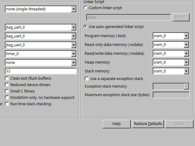
由於改用了SRAM,System Library Properties必須改成run在SRAM上。
若直接使用原本的test_checksum.c,執行後會出現以下錯誤訊息。
**** Build of configuration Debug for project blank_project_0 ****make -s all includes Compiling test_checksum.c../test_checksum.c: In function `main':../test_checksum.c:
52
: error: `ONCHIP_RAM_BASE' undeclared (first use in this function)../test_checksum.c:
52
: error: (Each undeclared identifier is reported only once../test_checksum.c:
52
: error: for each function it appears in.)make: ***
[
obj/test_checksum.o
]
Error
1
Build completed in
3.203
seconds
因為硬體沒使用on-chip memory,故register map也沒有ONCHIP_RAM_BASE這個macro,由於我們改用了SRAM,故將macro名稱改為SRAM_0_BASE。
/**/
/* base of onchip ram defined in system.h file */
2
/**/
/*alt_u8* buf = (alt_u8*) ONCHIP_RAM_BASE; */
3
alt_u8
*
buf
=
(alt_u8
*
)SRAM_0_BASE;
完整的test_checksum.c如下
/**/
/******************************************************************************2
 * Copyright (c) 2007 Altera Corporation, San Jose, California, USA. *
3
* All rights reserved. All use of this software and documentation is *4
* subject to the License Agreement located at the end of this file below. *5
 *******************************************************************************/
6
/**/
/* Simple C program that exercises the altera_avalon_checksum component by 7
* filling a memory buffer with test data and then configuring the 8
* altera_avalon_checksum to read back the data using the IOWR and IORD 9
* to directly write to the register locations as defined in the _regs.h 10
* file11
* 12
* Version History13
* BR 04/01/2007 Created14
* ATJ 04/12/2007 Add additional comments 15
* 16
*/
17
18
#include
<
stdio.h
>
19
#include
<
stdlib.h
>
20
#include
"
altera_avalon_checksum_regs.h
"
21
#include
"
system.h
"
22
#include
<
alt_types.h
>
23
24
25
/**/
/* Simple function that sets all contents of a buffer to the specified value. */
26
int
set_buf_val( alt_u8
*
buffer,
int
length, alt_u8 val )27
{28
int ret_code = 0;29
30

 /**//* Ok one byte at a time is not efficientC'est La Vie! */
31
32
while (length >= 0)33
{34
*(buffer + length) = val;35
if( *(buffer+length) != val )36
{37
ret_code = -1;38
 }
}39
length--;40
}41
return( ret_code );42
}
43
44
/**/
/* This program points the checksum component at a small buffer and45
* computes the checksum.46
*/
47
48
int
main()49
{50
/**//* Point the buffer at the base of the onchip ram.*/51
/**//* base of onchip ram defined in system.h file */52
/**//*alt_u8* buf = (alt_u8*) ONCHIP_RAM_BASE; */53
alt_u8* buf = (alt_u8*)SRAM_0_BASE;54
/**//* Set the length small, to start with. */55
int len = 12;56
int status;57
int result;58
59
60
/**//* Set the buffer to all 0xF0's. */61
printf( "Writing to test memory. \n");62
if( (set_buf_val( buf, len, 0xf0 )<0) )63
{64
printf( "Error: Could not pre-set buffer at %d.\n", (int) buf );65
return( -1 );66
}67
68
/**//* Setup the checksum component. */69
/**//* IORD and IOWR macros setup in alter_avalon_checksum_regs.h and io.h */70
71
/**//* Store the address (must be 32-bit word aligned address). */72
printf( "Writing to address register. \n");73
//IOWR_ALTERA_AVALON_CHECKSUM_ADDR( ALTERA_AVALON_CHECKSUM_INST_BASE, _RAM_BASE );74
IOWR_ALTERA_AVALON_CHECKSUM_ADDR( ALTERA_AVALON_CHECKSUM_INST_BASE, SRAM_0_BASE );75
/**//* Store the length in bytes (up to a 16-bit value). */76
printf( "Writing to length register. \n");77
IOWR_ALTERA_AVALON_CHECKSUM_LENGTH( ALTERA_AVALON_CHECKSUM_INST_BASE, len );78
/**//* Tell it to "go". */79
printf( "Writing to go bit in control register. \n");80
IOWR_ALTERA_AVALON_CHECKSUM_CTRL( ALTERA_AVALON_CHECKSUM_INST_BASE+ALTERA_AVALON_CHECKSUM_CTRL_GO_OFST, 81
ALTERA_AVALON_CHECKSUM_CTRL_GO_MSK);82
/**//* Polling loop waiting for the component to be done. */83
status = IORD_ALTERA_AVALON_CHECKSUM_STATUS( ALTERA_AVALON_CHECKSUM_INST_BASE );84
85
printf( "Polling for DONE bit in status register. . . \n");86
while( !(status & ALTERA_AVALON_CHECKSUM_STATUS_DONE_MSK) )87
{88
status = IORD_ALTERA_AVALON_CHECKSUM_STATUS( ALTERA_AVALON_CHECKSUM_INST_BASE );89
}90
printf( "Done bit asserted, exiting polling loop. \n");91
92
result = IORD_ALTERA_AVALON_CHECKSUM_RESULT( ALTERA_AVALON_CHECKSUM_INST_BASE );93
94
printf( "DoneResult = 0x%x.\n", (int) result );95
96
return 0;97
}
98
最後執行結果
完整程式碼下載
Altera原廠的altera_avalon_checksum.zip
Checksum Master on on-chip memory
Checksum Master on SRAM
Conclusion
凡是Altera原廠的範例,若要用在DE2,尤其是Nios II上,一定得改用DE2的reference design,這是跑不掉的。至於其他的修改,就得見招拆招了,畢竟DE2不是Altera原廠的版子。本文我們看到從軟體減少code size的方法,也看到從硬體從on-chip memory改用SRAM的方法。
See Also
(原創) 深入探討Altera的Checksum Master範例 (SOC) (SOPC Builder) (Nios II) (DE2)


 1万+
1万+

 被折叠的 条评论
为什么被折叠?
被折叠的 条评论
为什么被折叠?
 到【灌水乐园】发言


