


 本文介绍了一种简单有效的方法,通过电压转换将双极信号接入单极输入的ADC。详细解释了电路原理、关键公式及实际应用案例。
Voltage Translation for Analog to Digital Interface
孕龙逻辑分析仪 ZeroPlus Logic Analyzer
How to modify analog output range of Arduino Due
In today's microcontroller market, most of the Analog to Digital converters
are only able to accept voltages from the Vcc of the device to ground.
But what if you want to measure a bipolar signal?
This short tutorial plans to show you a simple but effective method
to interface a bipolar voltage to any single polarity input.
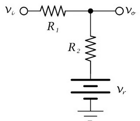
On the left is the ideal basic circuit for interfacing.
vi is the input voltage, vo is the voltage sent to the ADC,
vr is a reference voltage used for setting the center or zero input voltage,
and R1 and R2 are used for input scaling and current limiting
to bring the input voltage into the range of the ADC.
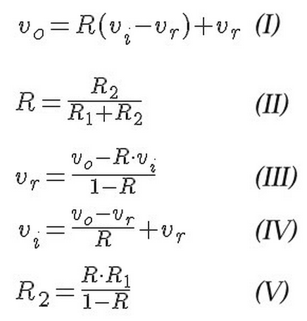
On the left are the 5 formulas needed to determine the values of vr and R2.
R1 will be chosen initially as we will see in an example below.
As you can see in formulas I,III,IV, and V,
the term R is the voltage divider ratio of the resistors calculated by formula II.
Now that I have my basic circuit, and the required formulas, let's now create a useful example.
In this example, my parameters will be as follows:
- Input impedance of at least 1Mohm.
- vin = +/- 12V
- vo = 0-5V
So when vin = 12v, vo = 5v
vin = -12v, vo = 0v
vin = 0v, vo = 2.5v
To begin, I need to calculate the value of R
This will be the scaling factor applied to the incoming voltage.
To do this, I take the vo range and divide it by the vin range. In this case,
R = 5/24 = .2083 [ 12v - -12v = 24v ]
Next I will calculate the value of R2.
Because I want an input impedance of at least 1Mohm, I will use 1M as R1.
Using formula V, the value for R2 is:
R2 = (R * R1)/(1-R) = (.2083 * 1M)/(1-.2083) = 208,300/.7917 = 263,104 ohms.
Next I need to calculate the value of vr.
Using the case of vin = 12, vo = 5, and using formula III:
vr = (vo - R * vi)/(1 - R) = (5 - .2083 * 12)/(1 - .2083) = 2.5004/.7917 = 3.158v
I now have the 3 values required for my design.
R1 = 1M
R2 = 263,104
vr = 3.158v
I can now plug these numbers into formula I
and calculate the three input voltages of +12, 0, and -12 and verify that the design is correct.
vo (vin=+12) = R(vi - vr) + vr = .2083(12 - 3.158) + 3.158 = 5.000
vo (vin= 0) = .2083(0 - 3.158) + 3.158 = 2.500
vo (vin=-12) = .2083(-12 - 3.158) + 3.158 = 0
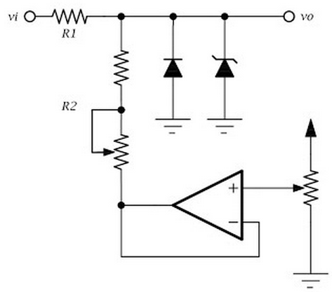 To the left is a practical circuit to interface to an ADC. The features are:
- A diode and zener diode used to protect the ADC input from overvoltage.
- R2 is composed of a fixed value, and a trim pot to dial in the correct value.
- A trim pot connected to the non inverting input of an op amp in a voltage follower configuration for setting vr.
vo (vin=+12) = R(vi - vr) + vr = .2083(12 - 3.158) + 3.158 = 5.000
vo (vin= 0) = .2083(0 - 3.158) + 3.158 = 2.500
vo (vin=-12) = .2083(-12 - 3.158) + 3.158 = 0
- A diode and zener diode used to protect the ADC input from overvoltage.
- R2 is composed of a fixed value, and a trim pot to dial in the correct value.
- A trim pot connected to the non inverting input of an op amp in a voltage follower configuration for setting vr.
To calibrate the circuit, adjust the op amp trim pot for an output voltage of vr as calculated above.
Next, input a voltage to vi and calculate what the vo should be,
and adjust the R2 trim pot until that voltage is achieved.
Now I have a working circuit, but the last thing to calculate is the maximum and minimum input voltages.
Note:
Generally, zener diodes will always have some current flow.
This will adversely affect the accuracy of the ADC measurements as well as the linearity.
A method of switching in the zener when max voltage is reached would be preferable,
but would increase the part count.
Now I have a working circuit, but the last thing to calculate is the maximum and minimum input voltages.
This will be determined by the two diodes and using formula IV.
The maximum input voltage will occur when the zener diode goes into breakdown regulation.
If we assume a zener voltage of 5.1v, the maximum input voltage is:
vi = ((vo - vr)/R) + vr = ((5.1 - 3.158)/.2083) + 3.158 = 12.481v
The minimum input voltage will occur when the diode is forward biased.
vi = ((vo - vr)/R) + vr = ((5.1 - 3.158)/.2083) + 3.158 = 12.481v
The minimum input voltage will occur when the diode is forward biased.
Assuming a forward voltage of 0.7v, the minimum input voltage is:
vi = ((-0.7 - 3.158)/.2083) + 3.158 = -15.363v
Effective input impedance can be calculated as follows:
zin = vin(R1 + R2)/(vin - vr)
This is a varying quantity depending on vin.
vi = ((-0.7 - 3.158)/.2083) + 3.158 = -15.363v
Effective input impedance can be calculated as follows:
zin = vin(R1 + R2)/(vin - vr)
This is a varying quantity depending on vin.


 1907
1907

 被折叠的 条评论
为什么被折叠?
被折叠的 条评论
为什么被折叠?
 到【灌水乐园】发言


