


 本文介绍了DG449双电源单刀双掷开关的特性,包括其低电阻、高精度信号切换能力及在电信通信和测试设备中的主要应用。此外,文章详细阐述了MOSFET对实现简单单刀双掷开关的作用,并提供了实际电路应用案例。
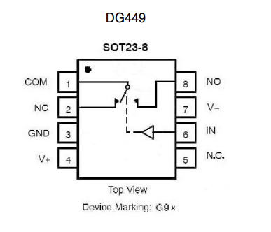
DESCRIPTION
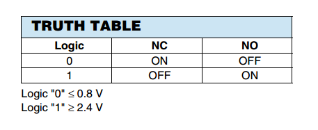
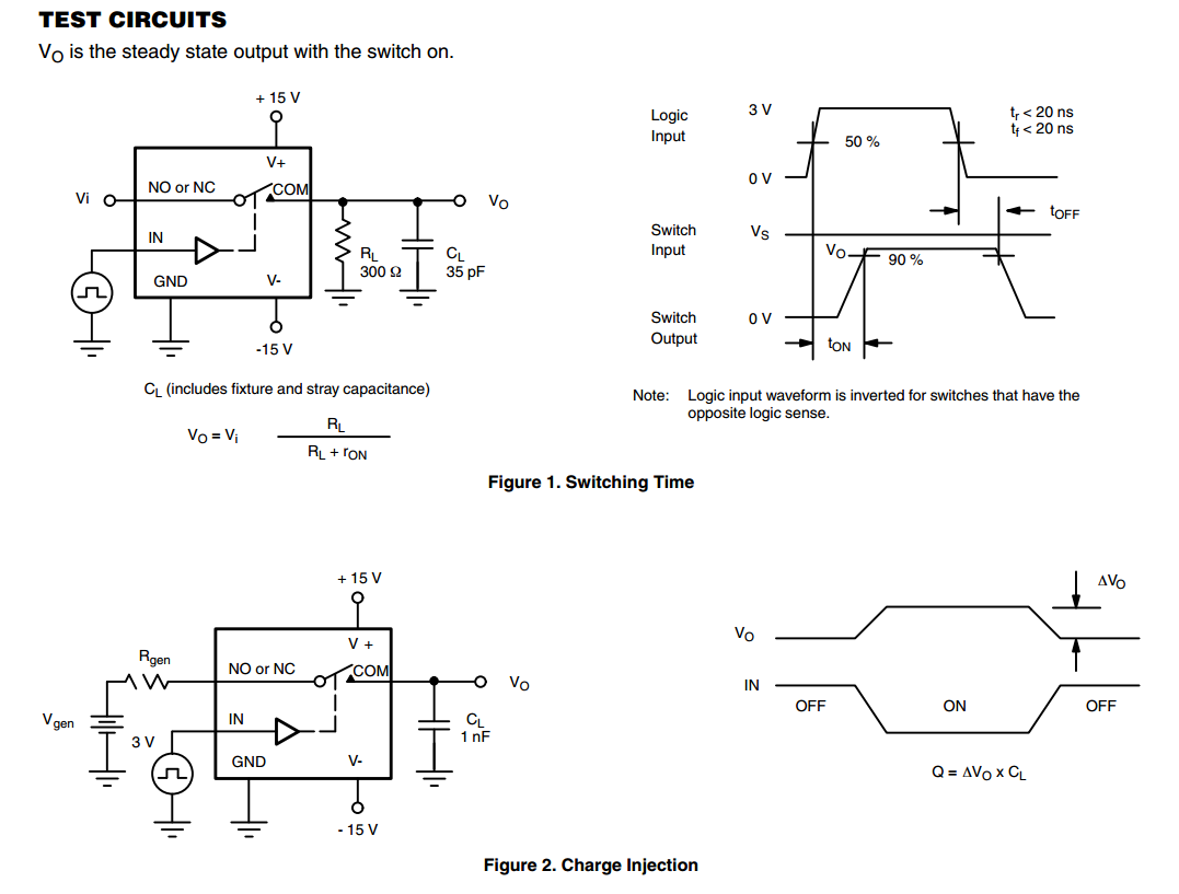
The DG449 is a dual supply single-pole/double-throw (SPDT) switches.
On resistance is 38 and flatness is 2.6 max over the specified analog signal range.
These analog switches were designed to provide high speed, low error switching of precision analog signals.
The primary application areas are in the routing and switching in telecommunications and test equipment.
Combining low power, low leakages, low on-resistance and small physical size,
the DG449 is also ideally suited for portable and battery powered industrial and military equipment.
The DG449 operates either from a single + 7 V to 36 V supply or from dual ± 4.5 V to ± 20 V supplies.
It is offered in the very popular, small SOT23-8 package.
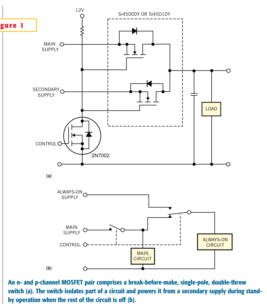
MOSFET pair makes simple SPDT switch
With an n- and p-channel MOSFET, you can easily implement a single-pole double-throw (SPDT) switch
to isolate part of a circuit and power it from a secondary supply for standby operation while the rest of the circuit is off (Figure 1).
By using a complementary pair, you can use a single control input for the MOSFETs.
An Si4501DY MOSFET in this topology exhibits less than a 0.1V drop at 5A
for the main element and contains both MOSFETs in an SO-8 package.
When the 2N7002 or similar control MOSFET ties the gates together
and pulls them to ground, the p-channel MOSFET is on.
Pulling the gates above the supply rail
by turning the 2N7002 off results in turning the n-channel MOSFET on.
Pulling the gate of the p-channel MOSFET above the source potential has no effect;
the MOSFET remains off with low leakage.
The resultant switch is a break-before-make configuration,
which is necessary to ensure that the secondary,
or always-on, supply never has to power the whole circuit.
However, due to the fast switching of the MOSFETs,
extra capacitance beyond normal design rules is probably unnecessary to maintain the operating voltage.
The arrangement of the n-channel device in the circuit ensures that the internal diode does not conduct while the subcircuit is isolated.
In this direction, the n-channel MOSFET also provides a fail-safe path for the circuit's power through the diode.
The forward voltage of the p-channel MOSFET's diode blocks any current from "back-feeding" the secondary supply,
assuming that the two supplies are close in voltage.
An example of an application for this circuit is the Advanced Configuration
and Power Interface in desktop computers providing instant-on and low power consumption in standby.
The main power supply is a high-power switching power supply,
and the secondary supply is a 60-Hz transformer with linear regulation. (DI #2451)


 506
506

 被折叠的 条评论
为什么被折叠?
被折叠的 条评论
为什么被折叠?
 到【灌水乐园】发言


