


 本文详细介绍了DDR4 SDRAM中的关键时序参数,包括激活、刷新、读取和写入操作的定时限制。例如,tRRD_S和tRRD_L规定了不同银行组间和同一银行组内连续激活命令的间隔,tFAW限制了连续激活命令的数量,tREFI定义了平均刷新间隔,CL和AL决定了读取和写入操作的延迟。这些参数对于理解和优化DDR4 SDRAM的性能至关重要。
DDR4 SDRAM - Understanding Timing Parameters
Introduction
There are a large number of timing parameters in the DDR standard, but when you work with DDR4 SDRAM you’ll often find yourself revisiting or reading about a handful of timing parameters more often than others. So, in this article we’ll examine only these frequently occurring timing parameters by looking at them in the context of a command.
These timing parameters are a hard thing to remember, they tend to slip out of your head. The accompanying article, Timing Parameter Cheat Sheet, can be used as a reference to recollect what a specific timing parameter means.
Note: All pictures below were taken from the DDR4 JEDEC specification and a Micron memory part spec. Links to them can be found in the Reference section.
ACTIVATE Timing
The ACTIVATE command is used to open a row within a bank. In Understanding the Basics we saw that every bank has a set of sense amps, so one row can remain active per bank. With ACTIVATE there are 3 timing parameters we should know about: tRRD_S, tRRD_L, tFAW
| Parameter | Function |
|---|---|
| tRRD_S | When issuing consecutive ACTIVATE commands to banks of different bank groups, the ACTIVATE commands have to be separated by tRRD_S (row-to-row delay–short) |
| tRRD_L | If the banks belong to the same bank group, their ACTIVATEs have to be separated by tRRD_L (row-to-row delay–long) |
| tFAW | Four Activate Window or sometimes also called Fifth Activate Window is a timing restriction. tFAW specifies a window within which only four activate commands can be issued. So, you can issue ACTIVATE commands back-to-back with tRRD_S between them, but once you have completed 4 activates you cannot issue another one until the tFAW window expires. |
Table 1: Activate command timing parameters
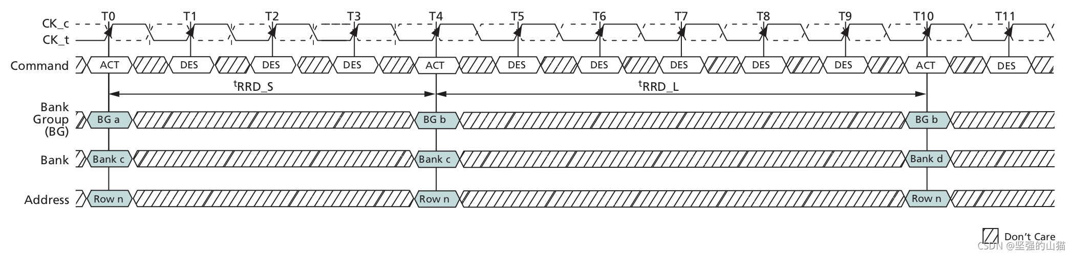
Figure 1: tRRD timing
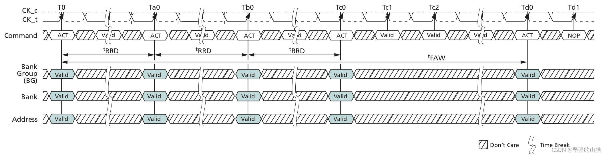
Figure 2: tFAW timing
REFRESH Timing
In order to ensure data stored in the SDRAM is not lost, the memory controller has to issue a REFRESH command at an average interval of tREFI. But before a REFRESH can be applied, all banks of the SDRAM have to be Precharged and idle for a minimum time of tRP(min). Once a REFRESH command is issued, there has to be a delay of tRFC(min) before the next valid command is issued (except DES command).
Notice how I mentioned that tREFI is the “average” interval between REFRESH commands. This is because you can push-out (or pull-in) a certain number of refresh commands and make up for it later. This mode was added to DDR4 to overcome the performance penalty due to refresh lockout at the higher densities. The number of refresh commands that can be postponed depends upon the Refresh Mode (1x, 2x or 4x) which can be set in the SDRAM’s Mode Register MR2.
| Parameter | Function |
|---|---|
| tREFI | The device requires REFRESH commands at an average interval of tREFI |
| tRP | Precharge time. The banks have to be precharged and idle for tRP before a REFRESH command can be applied |
| tRFC | Delay between the REFRESH command and the next valid command, except DES |
Table 2: Refresh command timing parameters
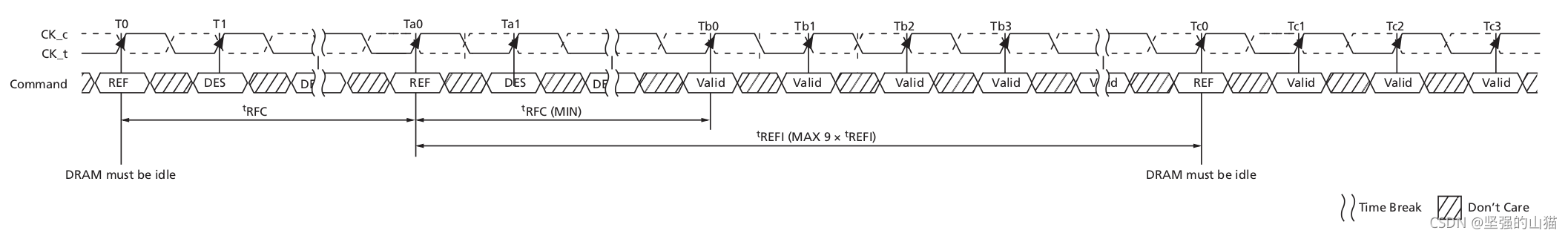
Figure 3: REFRESH timing
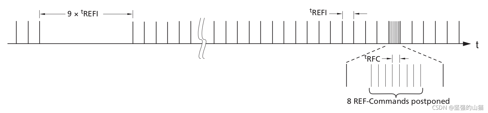
Figure 4: Postponing REFRESH command
READ Timing
The READ timing parameters can be broken up into 3 categories - Overall read timing, Clock-to-Strobe relationship and Data Strobe-to-Data relationship. Refer to DRAM-read-operation to understand the basics.
| Parameter | Function |
|---|---|
| Read Timing | |
| CL (CAS Latency) | CAS is the Column-Address-Strobe, i.e., when the column address is presented on the lines. CL is the delay, in clock cycles, between the internal READ command and the availability of the first bit of output data. It is defined in the MR0 mode register. SDRAM data sheets typically specific what the CL needs to be set for a particular frequency of operation. *See Fig 7* |
| AL (Additive Latency) | With AL, the device allows a READ command to be issued immediately after the ACTIVATE command. The command is held for the time of AL before it is issued inside the device. This feature is supported to sustain higher bandwidths/speeds in the device. |
| RL (Read Latency) | This is the overall read latency and is defined as RL = CL + AL |
| tCCD_S & tCCD_L | Bank accesses to different banks’ groups require less time delay between accesses than bank accesses to within the same bank’s group. Bank accesses to different bank groups require tCCD_S (or short) delay between commands while bank accesses within the same bank group require tCCD_L (or long) delay between commands. |
| Clock to Data Strobe relationship | |
| tDQSCK (MIN/MAX) | describes the allowed range for a rising data strobe edge relative to the clock CK_t, CK_c |
| tDQSCK | is the actual position of a rising strobe edge relative to CK_t, CK_c |
| tQSH | describes the data strobe high pulse width |
| tQSL | tQSL - describes the data strobe low pulse width. |
| Data Strobe to Data relationship | |
| tDQSQ | This describes the latest valid transition of the associated DQ data pins. From the picture below you’ll see that it is the time between when DQS transitions to the left edge of the DQ data-eye |
| tQH | Is the earliest invalid transition of the associated DQ pins. From the picture below you’ll see that it is the time from when DQS goes high to the right egdge of the DQ data-eye. |
Table 3: Read command timing parameters
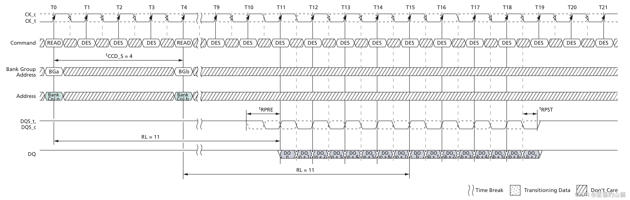
Figure 5: Consecutive READs to different Bank Groups. In this figure AL=0, CL = 11, so RL = 11. Notice how the read data burst (DQ bus) from the second READ immediately follows the first without any gap. Also notice tCCD_S between the 2 consecutive reads.
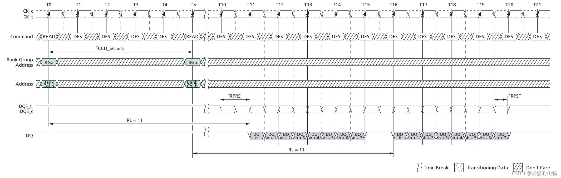
Figure 6: Non-Consecutive READs to different Bank Groups
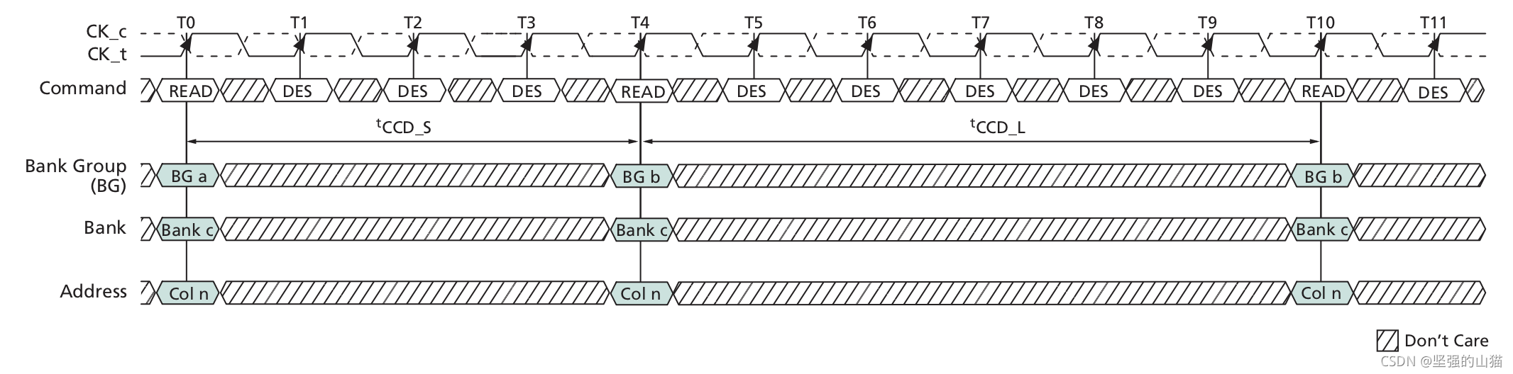
Figure 7: Illustration of tCCD_S and tCCD_L
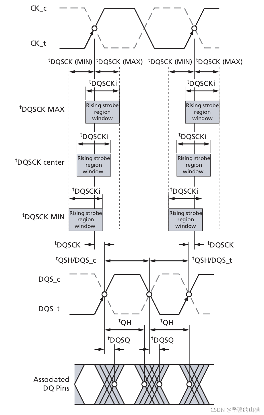
Figure 8: Illustrating CK-DQS and DQS-DQ relationships
WRITE Timing
Following similarly to the READ …
| Parameter | Function |
|---|---|
| Write timing | |
| CWL (CAS Write Latency) | CWL is the delay, in clock cycles, between the internal WRITE command and the availability of the first bit of input data. It is defined in Mode Register MR2. |
| AL (Additive Latency) | With AL, the device allows a WRITE command to be issued immediately after the ACTIVATE command. The command is held for the time of AL before it is issued inside the device. This feature is supported to sustain higher bandwidths/speeds in the device. |
| WL (Write Latency) | This is the overall write latency and is defined as WL = CWL + AL |
| tCCD_S & tCCD_L | Bank accesses to different banks’ groups require less time delay between accesses than bank accesses to within the same bank’s group. Bank accesses to different bank groups require tCCD_S (or short) delay between commands while bank accesses within the same bank group require tCCD_L (or long) delay between commands. |
| Clock to Data Strobe relationship | |
| tDQSS (MIN/MAX) | describes the allowed range for a rising data strobe edge relative to CK |
| tDQSS | is the actual position of a rising strobe edge relative to CK |
| tDQSH | describes the data strobe high pulse width |
| tDQSL | describes the data strobe low pulse width |
| tWPST | This of this as “post-write”. It is the time from when the last valid data strobe to when the strobe goes to HIGH, non-drive level. |
| tWPRE | This of this as “pre-write”. It is the time between when the data strobe goes from non-valid (HIGH) to valid (LOW, initial drive level). |
Table 4: Write command timing parameters
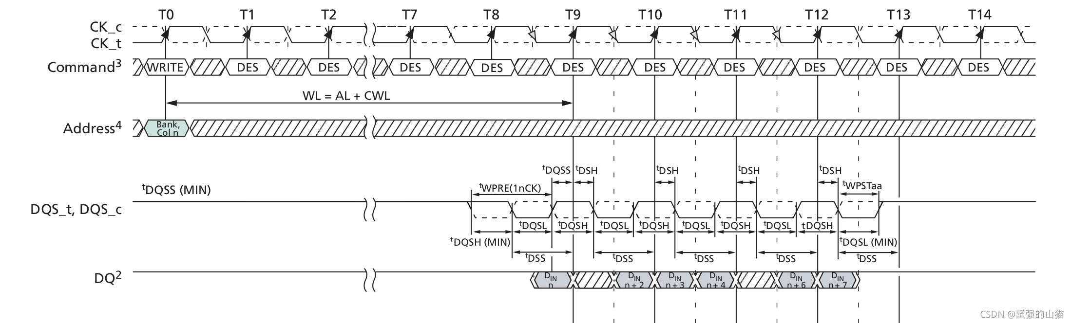
Figure 9: WRITE timing parameters
Mode Register Timing
SDRAMs provide a number of features, functions and settings which can be programmed using the 7 Mode Registers. These registers can be programmed using the MRS (Mode Register Set) command. The Mode Registers are set during initialization and thereafter they can be changed at any time during normal operation. Mode Register setting is governed by two timing parameters.
| Parameter | Function |
|---|---|
| tMRD | MRS command cycle time. It is the time required to complete the WRITE operation to the mode register and is the minimum time required between the two MRS commands shown in the tMRD Timing figure. |
| tMOD | is the minimum time required from an MRS command to a non MRS command, excluding DES. |
Table 5: Mode register command timing parameters
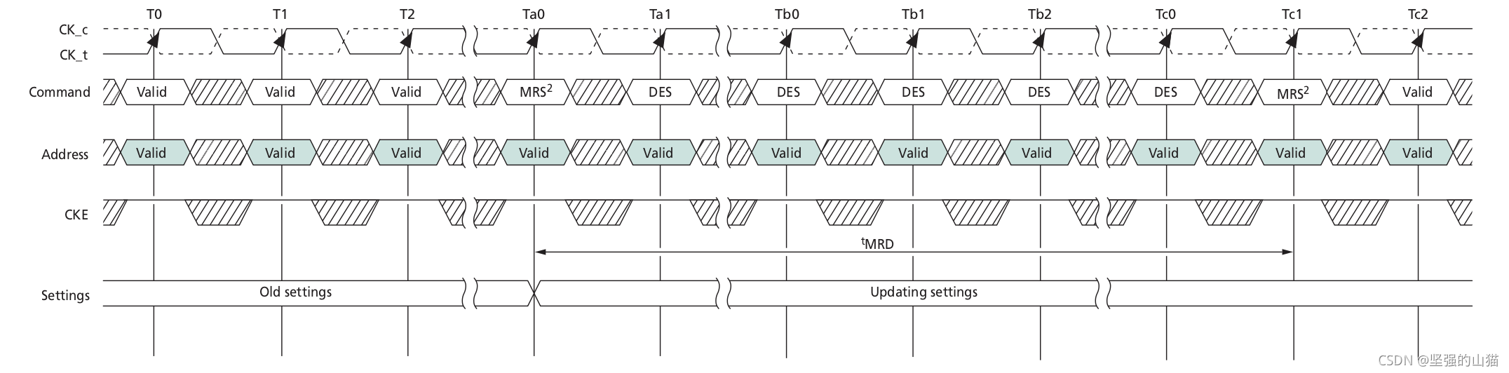
Figure 10: tMRD timing
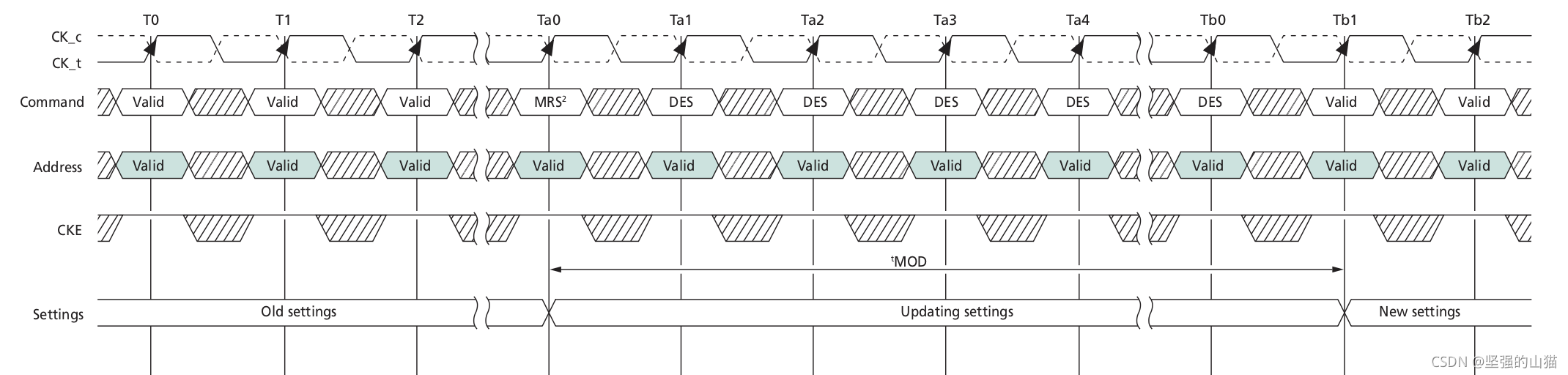
Figure 11: tMOD timing


 4180
4180

 被折叠的 条评论
为什么被折叠?
被折叠的 条评论
为什么被折叠?
 到【灌水乐园】发言


